DF2378BVFQ35V Renesas Electronics America, DF2378BVFQ35V Datasheet - Page 833
DF2378BVFQ35V
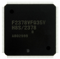
Manufacturer Part Number
DF2378BVFQ35V
Description
IC H8S/2378 MCU FLASH 144-LQFP
Manufacturer
Renesas Electronics America
Series
H8® H8S/2300r
Specifications of DF2378BVFQ35V
Core Processor
H8S/2000
Core Size
16-Bit
Speed
35MHz
Connectivity
I²C, IrDA, SCI, SmartCard
Peripherals
DMA, POR, PWM, WDT
Number Of I /o
97
Program Memory Size
512KB (512K x 8)
Program Memory Type
FLASH
Ram Size
32K x 8
Voltage - Supply (vcc/vdd)
3 V ~ 3.6 V
Data Converters
A/D 16x10b; D/A 6x8b
Oscillator Type
Internal
Operating Temperature
-20°C ~ 75°C
Package / Case
144-LQFP
For Use With
YLCDRSK2378 - KIT DEV EVAL H8S/2378 LCDYR0K42378FC000BA - KIT EVAL FOR H8S/2378HS0005KCU11H - EMULATOR E10A-USB H8S(X),SH2(A)EDK2378 - DEV EVAL KIT FOR H8S/2378
Lead Free Status / RoHS Status
Lead free / RoHS Compliant
Eeprom Size
-
Available stocks
Company
Part Number
Manufacturer
Quantity
Price
Company:

Part Number:
DF2378BVFQ35V
Manufacturer:
Renesas Electronics America
Quantity:
135
Company:
Part Number:
DF2378BVFQ35V
Manufacturer:
Renesas Electronics America
Quantity:
10 000


Section 15 Serial Communication Interface (SCI, IrDA)
When performing transfer using the DTC or DMAC, it is essential to set and enable the DTC or
DMAC before carrying out SCI setting. For details on the DTC or DMAC setting procedures,
refer to section 9, Data Transfer Controller (DTC) or section 7, DMA Controller (DMAC).
In receive operations, an RXI interrupt request is generated when the RDRF flag in SSR is set to
1. If the RXI request is designated beforehand as a DTC or DMAC activation source, the DTC or
DMAC will be activated by the RXI request, and transfer of the receive data will be carried out.
The RDRF flag is cleared to 0 automatically when data transfer is performed by the DTC or
DMAC. If an error occurs, an error flag is set but the RDRF flag is not. Consequently, the DTC or
DMAC is not activated, but instead, an ERI interrupt request is sent to the CPU. Therefore, the
error flag should be cleared.
15.10
Usage Notes
15.10.1 Module Stop Mode Setting
SCI operation can be disabled or enabled using the module stop control register. The initial setting
is for SCI operation to be halted. Register access is enabled by clearing module stop mode. For
details, refer to section 24, Power-Down Modes.
15.10.2 Break Detection and Processing
When framing error detection is performed, a break can be detected by reading the RxD pin value
directly. In a break, the input from the RxD pin becomes all 0s, and so the FER flag is set, and the
PER flag may also be set. Note that, since the SCI continues the receive operation after receiving a
break, even if the FER flag is cleared to 0, it will be set to 1 again.
15.10.3 Mark State and Break Sending
When TE is 0, the TxD pin is used as an I/O port whose direction (input or output) and level are
determined by DR and DDR. This can be used to set the TxD pin to mark state or send a break
during serial data transmission. To maintain the communication line at mark state until TE is set to
1, set both DDR and DR to 1. Since TE is cleared to 0 at this point, the TxD pin becomes an I/O
port, and 1 is output from the TxD pin. To send a break during serial transmission, first set DDR
to 1 and clear DR to 0, and then clear TE to 0. When TE is cleared to 0, the transmitter is
initialized regardless of the current transmission state, the TxD pin becomes an I/O port, and 0 is
output from the TxD pin.
Rev.7.00 Mar. 18, 2009 page 765 of 1136
REJ09B0109-0700
Related parts for DF2378BVFQ35V
Image
Part Number
Description
Manufacturer
Datasheet
Request
R

Part Number:
Description:
KIT STARTER FOR M16C/29
Manufacturer:
Renesas Electronics America
Datasheet:

Part Number:
Description:
KIT STARTER FOR R8C/2D
Manufacturer:
Renesas Electronics America
Datasheet:

Part Number:
Description:
R0K33062P STARTER KIT
Manufacturer:
Renesas Electronics America
Datasheet:

Part Number:
Description:
KIT STARTER FOR R8C/23 E8A
Manufacturer:
Renesas Electronics America
Datasheet:

Part Number:
Description:
KIT STARTER FOR R8C/25
Manufacturer:
Renesas Electronics America
Datasheet:

Part Number:
Description:
KIT STARTER H8S2456 SHARPE DSPLY
Manufacturer:
Renesas Electronics America
Datasheet:

Part Number:
Description:
KIT STARTER FOR R8C38C
Manufacturer:
Renesas Electronics America
Datasheet:

Part Number:
Description:
KIT STARTER FOR R8C35C
Manufacturer:
Renesas Electronics America
Datasheet:

Part Number:
Description:
KIT STARTER FOR R8CL3AC+LCD APPS
Manufacturer:
Renesas Electronics America
Datasheet:
Part Number:
Description:
KIT STARTER FOR RX610
Manufacturer:
Renesas Electronics America
Datasheet:

Part Number:
Description:
KIT STARTER FOR R32C/118
Manufacturer:
Renesas Electronics America
Datasheet:

Part Number:
Description:
KIT DEV RSK-R8C/26-29
Manufacturer:
Renesas Electronics America
Datasheet:

Part Number:
Description:
KIT STARTER FOR SH7124
Manufacturer:
Renesas Electronics America
Datasheet:

Part Number:
Description:
KIT STARTER FOR H8SX/1622
Manufacturer:
Renesas Electronics America
Datasheet:

Part Number:
Description:
KIT DEV FOR SH7203
Manufacturer:
Renesas Electronics America
Datasheet: