DF2378BVFQ35V Renesas Electronics America, DF2378BVFQ35V Datasheet - Page 298
DF2378BVFQ35V
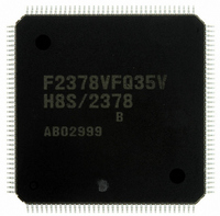
Manufacturer Part Number
DF2378BVFQ35V
Description
IC H8S/2378 MCU FLASH 144-LQFP
Manufacturer
Renesas Electronics America
Series
H8® H8S/2300r
Specifications of DF2378BVFQ35V
Core Processor
H8S/2000
Core Size
16-Bit
Speed
35MHz
Connectivity
I²C, IrDA, SCI, SmartCard
Peripherals
DMA, POR, PWM, WDT
Number Of I /o
97
Program Memory Size
512KB (512K x 8)
Program Memory Type
FLASH
Ram Size
32K x 8
Voltage - Supply (vcc/vdd)
3 V ~ 3.6 V
Data Converters
A/D 16x10b; D/A 6x8b
Oscillator Type
Internal
Operating Temperature
-20°C ~ 75°C
Package / Case
144-LQFP
For Use With
YLCDRSK2378 - KIT DEV EVAL H8S/2378 LCDYR0K42378FC000BA - KIT EVAL FOR H8S/2378HS0005KCU11H - EMULATOR E10A-USB H8S(X),SH2(A)EDK2378 - DEV EVAL KIT FOR H8S/2378
Lead Free Status / RoHS Status
Lead free / RoHS Compliant
Eeprom Size
-
Available stocks
Company
Part Number
Manufacturer
Quantity
Price
Company:

Part Number:
DF2378BVFQ35V
Manufacturer:
Renesas Electronics America
Quantity:
135
Company:
Part Number:
DF2378BVFQ35V
Manufacturer:
Renesas Electronics America
Quantity:
10 000


Section 6 Bus Controller (BSC)
Rev.7.00 Mar. 18, 2009 page 230 of 1136
REJ09B0109-0700
(Address shift size set to 8 bits)
DCTL
Figure 6.51 Example of DQMU and DQML Byte Control
This LSI
Notes: 1. Bank control is not available.
CS5 (SDRAMφ)
UCAS (DQMU)
LCAS (DQML)
2. The CKE and CS pins must be fixed to 1 when the power supply is input.
3. The CS pin must be fixed to 0 before accessing synchronous DRAM.
D15 to D0
CS2 (RAS)
CS3 (CAS)
I/O PORT
CS4 (WE)
OE (CKE)
A23
A21
A12
A11
A10
A9
A8
A7
A6
A5
A4
A3
A2
A1
64-Mbit synchronous DRAM
1 Mword × 16 bits × 4-bank configuration
8-bit column address
DQMU
RAS
CAS
WE
A13 (BS1)
A12 (BS0)
A11
A10
A9
A8
A7
A6
A5
A4
A3
A2
A1
A0
DQ15 to DQ0
CKE
CS
CLK
DQML
address: A13/A12
input: A11 to A0
Column address
input: A7 to A0
Row address
Bank select
Related parts for DF2378BVFQ35V
Image
Part Number
Description
Manufacturer
Datasheet
Request
R

Part Number:
Description:
KIT STARTER FOR M16C/29
Manufacturer:
Renesas Electronics America
Datasheet:

Part Number:
Description:
KIT STARTER FOR R8C/2D
Manufacturer:
Renesas Electronics America
Datasheet:

Part Number:
Description:
R0K33062P STARTER KIT
Manufacturer:
Renesas Electronics America
Datasheet:

Part Number:
Description:
KIT STARTER FOR R8C/23 E8A
Manufacturer:
Renesas Electronics America
Datasheet:

Part Number:
Description:
KIT STARTER FOR R8C/25
Manufacturer:
Renesas Electronics America
Datasheet:

Part Number:
Description:
KIT STARTER H8S2456 SHARPE DSPLY
Manufacturer:
Renesas Electronics America
Datasheet:

Part Number:
Description:
KIT STARTER FOR R8C38C
Manufacturer:
Renesas Electronics America
Datasheet:

Part Number:
Description:
KIT STARTER FOR R8C35C
Manufacturer:
Renesas Electronics America
Datasheet:

Part Number:
Description:
KIT STARTER FOR R8CL3AC+LCD APPS
Manufacturer:
Renesas Electronics America
Datasheet:
Part Number:
Description:
KIT STARTER FOR RX610
Manufacturer:
Renesas Electronics America
Datasheet:

Part Number:
Description:
KIT STARTER FOR R32C/118
Manufacturer:
Renesas Electronics America
Datasheet:

Part Number:
Description:
KIT DEV RSK-R8C/26-29
Manufacturer:
Renesas Electronics America
Datasheet:

Part Number:
Description:
KIT STARTER FOR SH7124
Manufacturer:
Renesas Electronics America
Datasheet:

Part Number:
Description:
KIT STARTER FOR H8SX/1622
Manufacturer:
Renesas Electronics America
Datasheet:

Part Number:
Description:
KIT DEV FOR SH7203
Manufacturer:
Renesas Electronics America
Datasheet: