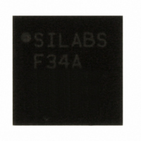
C8051F34A-GM Silicon Laboratories Inc, C8051F34A-GM Datasheet - Page 46

C8051F34A-GM
Manufacturer Part Number
C8051F34A-GM
Description
IC 8051 MCU 64K FLASH MEM 32-QFN
Manufacturer
Silicon Laboratories Inc
Series
C8051F34xr
Datasheet
1.C8051F349-GQ.pdf
(276 pages)
Specifications of C8051F34A-GM
Program Memory Type
FLASH
Program Memory Size
64KB (64K x 8)
Package / Case
32-QFN
Core Processor
8051
Core Size
8-Bit
Speed
48MHz
Connectivity
SMBus (2-Wire/I²C), SPI, UART/USART, USB
Peripherals
Brown-out Detect/Reset, POR, PWM, Temp Sensor, WDT
Number Of I /o
25
Ram Size
4.25K x 8
Voltage - Supply (vcc/vdd)
2.7 V ~ 3.6 V
Data Converters
A/D 17x10b
Oscillator Type
Internal
Operating Temperature
-40°C ~ 85°C
Processor Series
C8051F3x
Core
8051
Data Bus Width
8 bit
Data Ram Size
4352 B
Interface Type
I2C, SPI, UART
Maximum Clock Frequency
25 MHz
Number Of Programmable I/os
25
Number Of Timers
4
Operating Supply Voltage
2.7 V to 5.25 V
Maximum Operating Temperature
+ 85 C
Mounting Style
SMD/SMT
3rd Party Development Tools
KSK-SL-F34X, KSK-SL-TOOLSTICK, PK51, CA51, A51, ULINK2
Development Tools By Supplier
C8051F340DK
Minimum Operating Temperature
- 40 C
On-chip Adc
10 bit
Package
32QFN EP
Device Core
8051
Family Name
C8051F34x
Maximum Speed
48 MHz
Cpu Family
C8051F34x
Device Core Size
8b
Frequency (max)
48MHz
Total Internal Ram Size
4.25KB
# I/os (max)
25
Number Of Timers - General Purpose
4
Operating Supply Voltage (typ)
3.3/5V
Operating Supply Voltage (max)
5.25V
Operating Supply Voltage (min)
2.7V
Instruction Set Architecture
CISC
Operating Temp Range
-40C to 85C
Operating Temperature Classification
Industrial
Mounting
Surface Mount
Pin Count
32
Package Type
QFN EP
Lead Free Status / RoHS Status
Lead free / RoHS Compliant
For Use With
336-1748 - ADAPTER TOOLSTICK FOR C8051F34X
Eeprom Size
-
Lead Free Status / Rohs Status
Lead free / RoHS Compliant
Other names
336-1350-5
- Current page: 46 of 276
- Download datasheet (2Mb)
C8051F340/1/2/3/4/5/6/7/8/9/A/B/C/D
5.3.2. Tracking Modes
The AD0TM bit in register ADC0CN controls the ADC0 track-and-hold mode. In its default state, the ADC0
input is continuously tracked, except when a conversion is in progress. When the AD0TM bit is logic 1,
ADC0 operates in low-power track-and-hold mode. In this mode, each conversion is preceded by a track-
ing period of 3 SAR clocks (after the start-of-conversion signal). When the CNVSTR signal is used to initi-
ate conversions in low-power tracking mode, ADC0 tracks only when CNVSTR is low; conversion begins
on the rising edge of CNVSTR (see Figure 5.4). Tracking can also be disabled (shutdown) when the device
is in low power standby or sleep modes. Low-power track-and-hold mode is also useful when AMUX set-
tings are frequently changed, due to the settling time requirements described in
Time Requirements” on page
46
(AD0CM[2:0]=000, 001,010
Timer 1, Timer 3 Overflow
Write '1' to AD0BUSY,
(AD0CM[2:0]=100)
Timer 0, Timer 2,
Figure 5.4. 10-Bit ADC Track and Conversion Example Timing
SAR Clocks
SAR Clocks
SAR Clocks
AD0TM=1
AD0TM=0
011, 101)
AD0TM=1
AD0TM=0
CNVSTR
47.
Low Power
or Convert
Low Power
or Convert
Track or
Convert
A. ADC0 Timing for External Trigger Source
Track or Convert
B. ADC0 Timing for Internal Trigger Source
1
1
Track
2
2
Track
Rev. 1.3
3
3
4
4
1
Convert
5
5
2
6
6
3
7
7
4
8
Convert
8
Convert
Convert
5
9
9
6
10 11 12
10 11
7
8
9
13 14
Section “5.3.3. Settling
10 11
Low Power Mode
Track
Low Power
Mode
Track
Related parts for C8051F34A-GM
Image
Part Number
Description
Manufacturer
Datasheet
Request
R
Part Number:
Description:
SMD/C°/SINGLE-ENDED OUTPUT SILICON OSCILLATOR
Manufacturer:
Silicon Laboratories Inc
Part Number:
Description:
Manufacturer:
Silicon Laboratories Inc
Datasheet:
Part Number:
Description:
N/A N/A/SI4010 AES KEYFOB DEMO WITH LCD RX
Manufacturer:
Silicon Laboratories Inc
Datasheet:
Part Number:
Description:
N/A N/A/SI4010 SIMPLIFIED KEY FOB DEMO WITH LED RX
Manufacturer:
Silicon Laboratories Inc
Datasheet:
Part Number:
Description:
N/A/-40 TO 85 OC/EZLINK MODULE; F930/4432 HIGH BAND (REV E/B1)
Manufacturer:
Silicon Laboratories Inc
Part Number:
Description:
EZLink Module; F930/4432 Low Band (rev e/B1)
Manufacturer:
Silicon Laboratories Inc
Part Number:
Description:
I°/4460 10 DBM RADIO TEST CARD 434 MHZ
Manufacturer:
Silicon Laboratories Inc
Part Number:
Description:
I°/4461 14 DBM RADIO TEST CARD 868 MHZ
Manufacturer:
Silicon Laboratories Inc
Part Number:
Description:
I°/4463 20 DBM RFSWITCH RADIO TEST CARD 460 MHZ
Manufacturer:
Silicon Laboratories Inc
Part Number:
Description:
I°/4463 20 DBM RADIO TEST CARD 868 MHZ
Manufacturer:
Silicon Laboratories Inc
Part Number:
Description:
I°/4463 27 DBM RADIO TEST CARD 868 MHZ
Manufacturer:
Silicon Laboratories Inc
Part Number:
Description:
I°/4463 SKYWORKS 30 DBM RADIO TEST CARD 915 MHZ
Manufacturer:
Silicon Laboratories Inc
Part Number:
Description:
N/A N/A/-40 TO 85 OC/4463 RFMD 30 DBM RADIO TEST CARD 915 MHZ
Manufacturer:
Silicon Laboratories Inc
Part Number:
Description:
I°/4463 20 DBM RADIO TEST CARD 169 MHZ
Manufacturer:
Silicon Laboratories Inc


