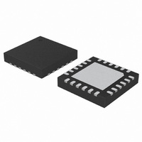
C8051F339-GM Silicon Laboratories Inc, C8051F339-GM Datasheet - Page 56

C8051F339-GM
Manufacturer Part Number
C8051F339-GM
Description
IC MCU 16K FLASH 24QFN
Manufacturer
Silicon Laboratories Inc
Series
C8051F33xr
Specifications of C8051F339-GM
Core Processor
8051
Core Size
8-Bit
Speed
25MHz
Connectivity
SMBus (2-Wire/I²C), SPI, UART/USART
Peripherals
POR, PWM, WDT
Number Of I /o
21
Program Memory Size
16KB (16K x 8)
Program Memory Type
FLASH
Ram Size
768 x 8
Voltage - Supply (vcc/vdd)
2.7 V ~ 3.6 V
Oscillator Type
Internal
Operating Temperature
-40°C ~ 85°C
Package / Case
24-QFN
Processor Series
C8051F3x
Core
8051
Data Bus Width
8 bit
Data Ram Size
768 B
Interface Type
I2C, SPI, UART
Maximum Clock Frequency
25 MHz
Number Of Programmable I/os
21
Number Of Timers
4
Operating Supply Voltage
2.7 V to 3.6 V
Maximum Operating Temperature
+ 85 C
Mounting Style
SMD/SMT
3rd Party Development Tools
KSK-SL-TOOLSTICK, PK51, CA51, A51, ULINK2
Development Tools By Supplier
C8051F336DK
Minimum Operating Temperature
- 40 C
Package
24QFN EP
Device Core
8051
Family Name
C8051F33x
Maximum Speed
25 MHz
Lead Free Status / RoHS Status
Lead free / RoHS Compliant
Eeprom Size
-
Data Converters
-
Lead Free Status / Rohs Status
Details
Other names
336-1426-5
- Current page: 56 of 226
- Download datasheet (2Mb)
C8051F336/7/8/9
10. Voltage Reference (C8051F336/8 only)
The Voltage reference multiplexer for the ADC is configurable to use an externally connected voltage refer-
ence, the on-chip reference voltage generator routed to the VREF pin, or the V
(see Figure 10.1). The REFSL bit in the Reference Control register (REF0CN, SFR Definition 10.1) selects
the reference source for the ADC. For an external source or the on-chip reference, REFSL should be set to
‘0’ to select the VREF pin. To use V
The BIASE bit enables the internal voltage bias generator, which is used by many of the analog peripherals
on the device. This bias is automatically enabled when any peripheral which requires it is enabled, and it
does not need to be enabled manually. The bias generator may be enabled manually by writing a ‘1’ to the
BIASE bit in register REF0CN. The electrical specifications for the voltage reference circuit are given in
Section “6. Electrical Characteristics” on page
The on-chip voltage reference circuit consists of a 1.2 V, temperature stable bandgap voltage reference
generator and a gain-of-two output buffer amplifier. The on-chip voltage reference can be driven on the
VREF pin by setting the REFBE bit in register REF0CN to a ‘1’. The maximum load seen by the VREF pin
must be less than 200 µA to GND. Bypass capacitors of 0.1 µF and 4.7 µF are recommended from the
VREF pin to GND. If the on-chip reference is not used, the REFBE bit should be cleared to ‘0’.
Important Note about the VREF Pin: When using either an external voltage reference or the on-chip ref-
erence circuitry, the VREF pin should be configured as an analog pin and skipped by the Digital Crossbar.
Refer to
of how to configure the pin in analog mode and to be skipped by the crossbar.
56
Section “20. Port Input/Output” on page 119
VDD
GND
Figure 10.1. Voltage Reference Functional Block Diagram
Recommended Bypass
4.7μF
R1
Capacitors
+
Reference
External
Voltage
Circuit
0.1μF
VREF
DD
as the reference source, REFSL should be set to ‘1’.
VDD
REF0CN
Rev.1.0
27.
0
1
IOSCE
for the location of the VREF pin, as well as details
N
Reference
REFBE
Internal
EN
EN
EN
Bias Generator
Temp Sensor
DD
To Analog Mux
(to ADC)
VREF
To ADC, IDAC,
Internal Oscillators
power supply voltage
Related parts for C8051F339-GM
Image
Part Number
Description
Manufacturer
Datasheet
Request
R
Part Number:
Description:
SMD/C°/SINGLE-ENDED OUTPUT SILICON OSCILLATOR
Manufacturer:
Silicon Laboratories Inc
Part Number:
Description:
Manufacturer:
Silicon Laboratories Inc
Datasheet:
Part Number:
Description:
N/A N/A/SI4010 AES KEYFOB DEMO WITH LCD RX
Manufacturer:
Silicon Laboratories Inc
Datasheet:
Part Number:
Description:
N/A N/A/SI4010 SIMPLIFIED KEY FOB DEMO WITH LED RX
Manufacturer:
Silicon Laboratories Inc
Datasheet:
Part Number:
Description:
N/A/-40 TO 85 OC/EZLINK MODULE; F930/4432 HIGH BAND (REV E/B1)
Manufacturer:
Silicon Laboratories Inc
Part Number:
Description:
EZLink Module; F930/4432 Low Band (rev e/B1)
Manufacturer:
Silicon Laboratories Inc
Part Number:
Description:
I°/4460 10 DBM RADIO TEST CARD 434 MHZ
Manufacturer:
Silicon Laboratories Inc
Part Number:
Description:
I°/4461 14 DBM RADIO TEST CARD 868 MHZ
Manufacturer:
Silicon Laboratories Inc
Part Number:
Description:
I°/4463 20 DBM RFSWITCH RADIO TEST CARD 460 MHZ
Manufacturer:
Silicon Laboratories Inc
Part Number:
Description:
I°/4463 20 DBM RADIO TEST CARD 868 MHZ
Manufacturer:
Silicon Laboratories Inc
Part Number:
Description:
I°/4463 27 DBM RADIO TEST CARD 868 MHZ
Manufacturer:
Silicon Laboratories Inc
Part Number:
Description:
I°/4463 SKYWORKS 30 DBM RADIO TEST CARD 915 MHZ
Manufacturer:
Silicon Laboratories Inc
Part Number:
Description:
N/A N/A/-40 TO 85 OC/4463 RFMD 30 DBM RADIO TEST CARD 915 MHZ
Manufacturer:
Silicon Laboratories Inc
Part Number:
Description:
I°/4463 20 DBM RADIO TEST CARD 169 MHZ
Manufacturer:
Silicon Laboratories Inc


