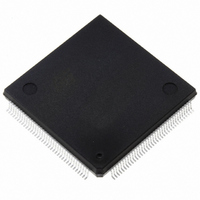
ST10R167-Q3 STMicroelectronics, ST10R167-Q3 Datasheet - Page 8

ST10R167-Q3
Manufacturer Part Number
ST10R167-Q3
Description
IC MCU 16BIT ROMLESS 144-PQFP
Manufacturer
STMicroelectronics
Series
ST10r
Datasheet
1.ST10R167-Q3.pdf
(63 pages)
Specifications of ST10R167-Q3
Core Processor
ST10
Core Size
16-Bit
Speed
25MHz
Connectivity
CAN, EBI/EMI, SSC, UART/USART
Peripherals
POR, PWM, WDT
Number Of I /o
111
Program Memory Type
ROMless
Ram Size
4K x 8
Voltage - Supply (vcc/vdd)
4.5 V ~ 5.5 V
Data Converters
A/D 16x10b
Oscillator Type
Internal
Operating Temperature
-40°C ~ 125°C
Package / Case
144-QFP
Processor Series
ST10R1x
Core
ST10
Data Bus Width
16 bit
Program Memory Size
32 KB
Data Ram Size
4 KB
Interface Type
CAN/SSC/USART
Maximum Clock Frequency
25 MHz
Number Of Programmable I/os
111
Number Of Timers
5
Maximum Operating Temperature
+ 125 C
Mounting Style
SMD/SMT
Minimum Operating Temperature
- 40 C
On-chip Adc
16-ch x 10-bit
Lead Free Status / RoHS Status
Lead free / RoHS Compliant
Eeprom Size
-
Program Memory Size
-
Lead Free Status / Rohs Status
Lead free / RoHS Compliant
Other names
497-2043
Available stocks
Company
Part Number
Manufacturer
Quantity
Price
Company:
Part Number:
ST10R167-Q3
Manufacturer:
ST
Quantity:
556
Company:
Part Number:
ST10R167-Q3
Manufacturer:
STMicroelectronics
Quantity:
10 000
Part Number:
ST10R167-Q3
Manufacturer:
ST
Quantity:
20 000
Company:
Part Number:
ST10R167-Q3/TR
Manufacturer:
STMicroelectronics
Quantity:
10 000
Company:
Part Number:
ST10R167-Q3B0
Manufacturer:
ST
Quantity:
1 343
Part Number:
ST10R167-Q3B0
Manufacturer:
ST
Quantity:
20 000
ST10R167
II - PIN DATA (continued)
Table 1 : Pin list (continued)
8/63
READY/READY
P0H.1 - P0H.7
P1H.0 - P1H.7
P0L.0 - P0L.7
P1L.0 - P1L.7
WR/WRL
Symbol
XTAL1
XTAL2
RSTIN
P0H.0
ALE
EA
100 - 107
128 - 135
118 - 125
111 - 117
108
132
133
134
135
138
137
140
Pin
96
97
98
99
Type
I/O
I/O
O
O
O
I
I
I
I
I
I
I
I
External Memory Write Strobe. In WR-mode this pin is activated for every
external data write access. In WRL-mode this pin is activated for low byte
data write accesses on a 16-bit bus, and for every data write access on an
8-bit bus. See WRCFG in register SYSCON for mode selection.
Ready Input. The active level is programmable. When the Ready function
is enabled, the selected inactive level at this pin during an external mem-
ory access will force the insertion of memory cycle time waitstates until
the pin returns to the selected active level.
Address Latch Enable Output. Can be used for latching the address into
external memory or an address latch in the multiplexed bus modes.
External Access Enable pin. A low level at this pin during and after Reset
forces the ST10R167 to begin instruction execution out of external mem-
ory. A high level forces execution out of the internal Flash Memory.
Port 0 consists of the two 8-bit bidirectional I/O ports P0L and P0H. It is
bit-wise programmable for input or output via direction bits. For a pin con-
figured as input, the output driver is put into high-impedance state. In case
of an external bus configuration, Port 0 serves as the address (A) and
address/data (AD) bus in multiplexed bus modes and as the data (D) bus
in demultiplexed bus modes.
Demultiplexed bus modes:
Data Path Width : 8-bit
P0L.0 – P0L.7
P0H.0 – P0H.7
Multiplexed bus modes:
Data Path Width : 8-bit
P0L.0 – P0L.7
P0H.0 – P0H.7
Port 1 consists of the two 8-bit bidirectional I/O ports P1L and P1H. It is
bit-wise programmable for input or output via direction bits. For a pin con-
figured as input, the output driver is put into high-impedance state. Port 1
is used as the 16-bit address bus (A) in demultiplexed bus modes and
also after switching from a demultiplexed bus mode to a multiplexed bus
mode.
The following PORT1 pins also serve for alternate functions:
P1H.4
P1H.5
P1H.6
P1H.7
Input to the oscillator amplifier and input to the internal clock generator
Output of the oscillator amplifier circuit.
To clock the device from an external source, drive XTAL1, while leaving
XTAL2 unconnected. Minimum and maximum high/low and rise/fall times
specified in the AC Characteristics must be observed.
Reset Input with Schmitt-Trigger characteristics. A low level at this pin for
a specified duration while the oscillator is running resets the ST10R167.
An internal pullup resistor permits power-on reset using only a capacitor
connected to V
In bidirectional reset mode (enabled by setting bit BDRSTEN in SYSCON
register), the RSTIN line is pulled low for the duration of the internal reset
sequence.
CC24IO
CC25IO
CC26IO
CC27IO
SS
.
: D0 – D7
: I/O
: AD0 – AD7
: A8 - A15
CAPCOM2: CC24 Capture Input
CAPCOM2: CC25 Capture Input
CAPCOM2: CC26 Capture Input
CAPCOM2: CC27 Capture Input
Function
16-bit
D0 - D7
D8 - D15
16-bit
AD0 - AD7
AD8 - AD15


