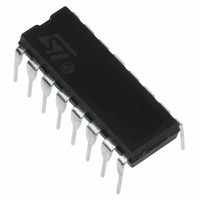
ST62T00CB6 STMicroelectronics, ST62T00CB6 Datasheet - Page 26

ST62T00CB6
Manufacturer Part Number
ST62T00CB6
Description
IC MCU 8BIT OTP 1K 16-PDIP
Manufacturer
STMicroelectronics
Series
ST6r
Specifications of ST62T00CB6
Core Processor
ST6
Core Size
8-Bit
Speed
8MHz
Peripherals
LVD, POR, WDT
Number Of I /o
9
Program Memory Size
1KB (1K x 8)
Program Memory Type
OTP
Ram Size
64 x 8
Voltage - Supply (vcc/vdd)
3 V ~ 6 V
Data Converters
A/D 4x8b
Oscillator Type
Internal
Operating Temperature
-40°C ~ 85°C
Package / Case
16-DIP (0.300", 7.62mm)
Controller Family/series
ST6
No. Of I/o's
9
Ram Memory Size
64Byte
Cpu Speed
8MHz
No. Of Timers
1
Rohs Compliant
Yes
Processor Series
ST62T0x
Core
ST6
Data Bus Width
8 bit
Data Ram Size
64 B
Maximum Clock Frequency
8 MHz
Number Of Programmable I/os
9
Number Of Timers
2
Operating Supply Voltage
3 V to 6 V
Maximum Operating Temperature
+ 85 C
Mounting Style
Through Hole
Development Tools By Supplier
ST622XC-KIT/110, ST62GP-EMU2, ST62E2XC-EPB/110, ST62E6XC-EPB/US, STREALIZER-II
Minimum Operating Temperature
- 40 C
On-chip Adc
8 bit
Cpu Family
ST6
Device Core Size
8b
Frequency (max)
8MHz
Total Internal Ram Size
64Byte
# I/os (max)
9
Number Of Timers - General Purpose
1
Operating Supply Voltage (typ)
3.3/5V
Operating Supply Voltage (max)
6V
Operating Supply Voltage (min)
3V
Instruction Set Architecture
CISC
Operating Temp Range
-40C to 85C
Operating Temperature Classification
Industrial
Mounting
Through Hole
Pin Count
16
Package Type
PDIP
Lead Free Status / RoHS Status
Lead free / RoHS Compliant
Eeprom Size
-
Connectivity
-
Lead Free Status / Rohs Status
In Transition
Other names
497-2093-5
Available stocks
Company
Part Number
Manufacturer
Quantity
Price
Company:
Part Number:
ST62T00CB6
Manufacturer:
MICRON
Quantity:
1 450
Company:
Part Number:
ST62T00CB6
Manufacturer:
STMicroelectronics
Quantity:
135
ST62T00C/T01C ST62T03C/E01C
3.4 INTERRUPTS
The CPU can manage four Maskable Interrupt
sources, in addition to a Non Maskable Interrupt
source (top priority interrupt). Each source is asso-
ciated with a specific Interrupt Vector which con-
tains a Jump instruction to the associated interrupt
service routine. These vectors are located in Pro-
gram space (see Table 6).
When an interrupt source generates an interrupt
request, and interrupt processing is enabled, the
PC register is loaded with the address of the inter-
rupt vector (i.e. of the Jump instruction), which
then causes a Jump to the relevant interrupt serv-
ice routine, thus servicing the interrupt.
Interrupt sources are linked to events either on ex-
ternal pins, or on chip peripherals. Several events
can be ORed on the same interrupt source, and
relevant flags are available to determine which
event triggered the interrupt.
The Non Maskable Interrupt request has the high-
est priority and can interrupt any interrupt routine
at any time; the other four interrupts cannot inter-
rupt each other. If more than one interrupt request
is pending, these are processed by the processor
core according to their priority level: source #1 has
the higher priority while source #4 the lower. The
priority of each interrupt source is fixed.
Table 6. Interrupt Vector Map
3.4.1 Interrupt request
All interrupt sources but the Non Maskable Inter-
rupt source can be disabled by setting accordingly
the GEN bit of the Interrupt Option Register (IOR).
This GEN bit also defines if an interrupt source, in-
cluding the Non Maskable Interrupt source, can re-
start the MCU from STOP/WAIT modes.
Interrupt request from the Non Maskable Interrupt
source #0 is latched by a flip flop which is automat-
26/70
26
Interrupt source #0
Interrupt source #1
Interrupt source #2
Interrupt source #3
Interrupt source #4
Interrupt Source
Priority
1
2
3
4
5
(FFCh-FFDh)
(FF6h-FF7h)
(FF4h-FF5h)
(FF2h-FF3h)
(FF0h-FF1h)
Vector Address
ically reset by the core at the beginning of the non-
maskable interrupt service routine.
Interrupt request from source #1 can be config-
ured either as edge or level sensitive by setting ac-
cordingly the LES bit of the Interrupt Option Regis-
ter (IOR).
Interrupt request from source #2 are always edge
sensitive. The edge polarity can be configured by
setting accordingly the ESB bit of the Interrupt Op-
tion Register (IOR).
Interrupt request from sources #3 & #4 are level
sensitive.
In edge sensitive mode, a latch is set when a edge
occurs on the interrupt source line and is cleared
when the associated interrupt routine is started.
So, the occurrence of an interrupt can be stored,
until completion of the running interrupt routine be-
fore being processed. If several interrupt requests
occurs before completion of the running interrupt
routine, only the first request is stored.
Storage of interrupt requests is not available in lev-
el sensitive mode. To be taken into account, the
low level must be present on the interrupt pin when
the MCU samples the line after instruction execu-
tion.
At the end of every instruction, the MCU tests the
interrupt lines: if there is an interrupt request the
next instruction is not executed and the appropri-
ate interrupt service routine is executed instead.
Table 7. Interrupt Option Register Description
GEN
ESB
LES
OTHERS
SET
CLEARED
SET
CLEARED
SET
CLEARED
NOT USED
Enable all interrupts
Disable all interrupts
Rising edge mode on inter-
rupt source #2
Falling edge mode on inter-
rupt source #2
Level-sensitive mode on in-
terrupt source #1
Falling edge mode on inter-
rupt source #1


