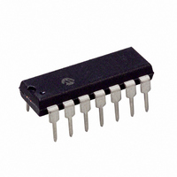
PIC16F636-I/P Microchip Technology, PIC16F636-I/P Datasheet - Page 71

PIC16F636-I/P
Manufacturer Part Number
PIC16F636-I/P
Description
IC MCU FLASH 2KX14 14DIP
Manufacturer
Microchip Technology
Series
PIC® 16Fr
Datasheets
1.PIC16F616T-ISL.pdf
(8 pages)
2.PIC12F635-ISN.pdf
(234 pages)
3.PIC16F636-ISL.pdf
(8 pages)
4.PIC16F636-ISL.pdf
(4 pages)
5.PIC16F636-IST.pdf
(196 pages)
Specifications of PIC16F636-I/P
Program Memory Type
FLASH
Program Memory Size
3.5KB (2K x 14)
Package / Case
14-DIP (0.300", 7.62mm)
Core Processor
PIC
Core Size
8-Bit
Speed
20MHz
Peripherals
Brown-out Detect/Reset, LVD, POR, WDT
Number Of I /o
11
Ram Size
128 x 8
Voltage - Supply (vcc/vdd)
2 V ~ 5.5 V
Oscillator Type
Internal
Operating Temperature
-40°C ~ 85°C
Processor Series
PIC16F
Core
PIC
Data Bus Width
8 bit
Data Ram Size
128 B
Interface Type
RS- 232/SPI/USB
Maximum Clock Frequency
20 MHz
Number Of Programmable I/os
12
Number Of Timers
2
Operating Supply Voltage
2 V to 5.5 V
Maximum Operating Temperature
+ 85 C
Mounting Style
Through Hole
3rd Party Development Tools
52715-96, 52716-328, 52717-734
Development Tools By Supplier
PG164130, DV164035, DV244005, DV164005, PG164120
Minimum Operating Temperature
- 40 C
On-chip Adc
8 bit
Lead Free Status / RoHS Status
Lead free / RoHS Compliant
For Use With
AC164039 - MODULE SKT PROMATE II 20DIP/SOICAC162057 - MPLAB ICD 2 HEADER 14DIPACICE0207 - MPLABICE 14P 300 MIL ADAPTER
Eeprom Size
-
Data Converters
-
Connectivity
-
Lead Free Status / Rohs Status
Lead free / RoHS Compliant
7.7
Response time is the minimum time, after selecting a
new reference voltage or input source, before the
comparator output is ensured to have a valid level. If
the internal reference is changed, the maximum delay
of the internal voltage reference must be considered
when using the comparator outputs. Otherwise, the
maximum delay of the comparators should be used
(Table 15-7).
7.8
The comparators and voltage reference, if enabled
before entering Sleep mode, remain active during
Sleep. This results in higher Sleep currents than shown
in the power-down specifications. The additional
current consumed by the comparator and the voltage
reference is shown separately in the specifications. To
minimize power consumption while in Sleep mode, turn
off the comparator, CM<2:0> = 111 and voltage
reference, VRCON<7> = 0.
REGISTER 7-3:
© 2005 Microchip Technology Inc.
Comparator Response Time
Operation During Sleep
bit 7
bit 6
bit 5
bit 4
bit 3-0
VRCON – VOLTAGE REFERENCE CONTROL REGISTER (ADDRESS: 99h)
bit 7
VREN: CV
1 = CV
0 = CV
Unimplemented: Read as ‘0’
VRR: CV
1 = Low range
0 = High range
Unimplemented: Read as ‘0’
VR<3:0>: CV
When VRR = 1:
CV
When VRR = 0:
CV
Legend:
R = Readable bit
- n = Value at POR
R/W-0
VREN
REF
REF
REF
REF
= (VR<3:0>/24) * V
= V
REF
REF
DD
circuit powered on
circuit powered down, no I
/4 + (VR<3:0>/32) * V
Range Selection bit
REF
Enable bit
U-0
—
Value Selection bits 0
R/W-0
PIC12F635/PIC16F636/639
VRR
DD
Preliminary
W = Writable bit
‘1’ = Bit is set
DD
DD
R/W-0
—
While the comparator is enabled during Sleep, an
interrupt will wake-up the device. If the GIE bit
(INTCON<7>) is set, the device will jump to the
interrupt vector (0004h) and if clear, continues
execution with the next instruction. If the device wakes
up from Sleep, the contents of the CMCON0, CMCON1
and VRCON registers are not affected.
7.9
A device Reset forces the CMCON0, CMCON1 and
VRCON registers to their Reset states. This forces the
comparator module to be in the Comparator Reset
mode, CM<2:0> = 000 and the voltage reference to its
OFF state. Thus, all potential inputs are analog inputs
with the comparator and voltage reference disabled to
consume the smallest current possible.
drain and CV
VR<3:0>
Effects of a Reset
R/W-0
U = Unimplemented bit, read as ‘0’
‘0’ = Bit is cleared
VR3
15
REF
= V
R/W-0
SS
VR2
x = Bit is unknown
R/W-0
VR1
DS41232B-page 69
R/W-0
VR0
bit 0


