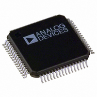
ADUC7128BSTZ126-RL Analog Devices Inc, ADUC7128BSTZ126-RL Datasheet - Page 55

ADUC7128BSTZ126-RL
Manufacturer Part Number
ADUC7128BSTZ126-RL
Description
IC DAS MCU ARM7 ADC/DDS 64-LQFP
Manufacturer
Analog Devices Inc
Series
MicroConverter® ADuC7xxxr
Datasheet
1.EVAL-ADUC7128QSPZ.pdf
(92 pages)
Specifications of ADUC7128BSTZ126-RL
Core Size
16/32-Bit
Program Memory Size
126KB (126K x 8)
Core Processor
ARM7
Speed
41.78MHz
Connectivity
I²C, SPI, UART/USART
Peripherals
PLA, POR, PWM, PSM, Temp Sensor, WDT
Number Of I /o
28
Program Memory Type
FLASH
Ram Size
8K x 8
Voltage - Supply (vcc/vdd)
3 V ~ 3.6 V
Data Converters
A/D 10x12b; D/A 1x10b
Oscillator Type
Internal
Operating Temperature
-40°C ~ 125°C
Package / Case
64-LQFP
Controller Family/series
(ARM7) ADUC
No. Of I/o's
40
Cpu Speed
41.78MHz
No. Of Timers
5
Digital Ic Case Style
LQFP
Embedded Interface Type
I2C, SPI, UART
Rohs Compliant
Yes
Lead Free Status / RoHS Status
Lead free / RoHS Compliant
For Use With
EVAL-ADUC7128QSPZ - KIT DEV FOR ADUC7128
Eeprom Size
-
Lead Free Status / RoHS Status
Lead free / RoHS Compliant, Lead free / RoHS Compliant
Other names
ADUC7128BSTZ126-RLTR
Available stocks
Company
Part Number
Manufacturer
Quantity
Price
Company:
Part Number:
ADUC7128BSTZ126-RL
Manufacturer:
Analog Devices Inc
Quantity:
10 000
QENCLR Register
Name
QENCLR
Writing any value to the QENCLR register clears the QENVAL
register to 0x0000. The bits in this register are undefined.
QENSET Register
Name
QENSET
Writing any value to the QENSET register loads the QENVAL
register with the value in QENDAT. The bits in this register are
undefined.
Note that the interrupt conditions are OR’ e d together to form
one interrupt to the interrupt controller. The interrupt service
routine should check the QENSTA register to find out the cause
of the interrupt.
•
•
•
The counter with the quadrature encoder is gray encoded to
ensure reliable data transfer across clock boundaries. When an
underflow or overflow occur, the count value does not jump to
the other end of the scale; instead, the direction of count changes.
When this happens, the value in QENDAT is subtracted from the
value derived from the gray count.
When the value in QENDAT changes, the value read back from
QENVAL changes. However, the gray encoded value does not
change. This only occurs after an underflow or overflow. If the
value in QENDAT changes, there must be a write to QENSET
or QENCLR to ensure a valid number is read back from QENVAL.
The S1 and S2 inputs appear as the QENS1 and QENS2
inputs in the GPIO list.
The motor speed can be measured by using the capture
facility in Timer0 or Timer1.
An overflow of either timer can be checked by using an ISR
or by checking IRQSIG.
Address
0xFFFF0F14
Address
0xFFFF0F18
Default Value
0x00000000
Default Value
0x00000000
Access
R/W
Access
R/W
Rev. 0 | Page 55 of 92
GENERAL-PURPOSE I/O
The ADuC7128/ADuC7129 provide 40 general-purpose,
bidirectional I/O (GPIO) pins. All I/O pins are 5 V tolerant,
meaning that the GPIOs support an input voltage of 5 V. In
general, many of the GPIO pins have multiple functions (see
Table 70). By default, the GPIO pins are configured in GPIO mode.
All GPIO pins have an internal pull-up resistor (of about 100 kΩ)
and their drive capability is 1.6 mA. Note that a maximum of
20 GPIO can drive 1.6 mA at the same time. The following GPIOs
have programmable pull-up: P0.0, P0.4, P0.5, P0.6, P0.7, and
the eight GPIOs of P1.
The 40 GPIOs are grouped in five ports: Port 0 to Port 4. Each
port is controlled by four or five MMRs, with x representing the
port number.
GPxCON Register
Name
GP0CON
GP1CON
GP2CON
GP3CON
GP4CON
Note that the kernel changes P0.6 from its default configuration
at reset ( MRST ) to GPIO mode. If MRST is used for external
circuitry, an external pull-up resistor should be used to ensure
that the level on P0.6 does not drop when the kernel switches
mode. Otherwise, P0.6 goes low for the reset period. For example,
if MRST is required for power-down, it can be reconfigured in
GP0CON MMR.
The input level of any GPIO can be read at any time in the
GPxDAT MMR, even when the pin is configured in a mode
other than GPIO. The PLA input is always active.
When the ADuC7128/ADuC7129 enter a power-saving mode,
the GPIO pins retain their state.
GPxCON is the Port x control register, and it selects the
function of each pin of Port x, as described in Table 70.
Address
0xFFFF0D00
0xFFFF0D04
0xFFFF0D08
0xFFFF0D0C
0xFFFF0D10
ADuC7128/ADuC7129
Default Value
0x00000000
0x00000000
0x00000000
0x11111111
0x00000000
Access
R/W
R/W
R/W
R/W
R/W


