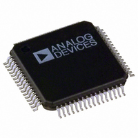
ADUC7128BSTZ126-RL Analog Devices Inc, ADUC7128BSTZ126-RL Datasheet - Page 34

ADUC7128BSTZ126-RL
Manufacturer Part Number
ADUC7128BSTZ126-RL
Description
IC DAS MCU ARM7 ADC/DDS 64-LQFP
Manufacturer
Analog Devices Inc
Series
MicroConverter® ADuC7xxxr
Datasheet
1.EVAL-ADUC7128QSPZ.pdf
(92 pages)
Specifications of ADUC7128BSTZ126-RL
Core Size
16/32-Bit
Program Memory Size
126KB (126K x 8)
Core Processor
ARM7
Speed
41.78MHz
Connectivity
I²C, SPI, UART/USART
Peripherals
PLA, POR, PWM, PSM, Temp Sensor, WDT
Number Of I /o
28
Program Memory Type
FLASH
Ram Size
8K x 8
Voltage - Supply (vcc/vdd)
3 V ~ 3.6 V
Data Converters
A/D 10x12b; D/A 1x10b
Oscillator Type
Internal
Operating Temperature
-40°C ~ 125°C
Package / Case
64-LQFP
Controller Family/series
(ARM7) ADUC
No. Of I/o's
40
Cpu Speed
41.78MHz
No. Of Timers
5
Digital Ic Case Style
LQFP
Embedded Interface Type
I2C, SPI, UART
Rohs Compliant
Yes
Lead Free Status / RoHS Status
Lead free / RoHS Compliant
For Use With
EVAL-ADUC7128QSPZ - KIT DEV FOR ADUC7128
Eeprom Size
-
Lead Free Status / RoHS Status
Lead free / RoHS Compliant, Lead free / RoHS Compliant
Other names
ADUC7128BSTZ126-RLTR
Available stocks
Company
Part Number
Manufacturer
Quantity
Price
Company:
Part Number:
ADUC7128BSTZ126-RL
Manufacturer:
Analog Devices Inc
Quantity:
10 000
ADuC7128/ADuC7129
Table 33. ADCCON MMR Bit Designations
Bit
12:10
9:8
7
6
5
4:3
2:0
Value
000
001
010
011
100
101
00
01
10
11
00
01
10
11
000
001
010
011
100
101
110
Other
Enable Conversion.
Reserved.
PLA Conversion.
Description
ADC Clock Speed (fADC = F
fADC/1. This divider is provided to obtain 1 MSPS ADC with an external clock <41.78 MHz.
fADC/2 (default value).
fADC/4.
fADC/8.
fADC/16.
fADC/32.
ADC Acquisition Time (Number of ADC Clocks).
2 clocks.
4 clocks.
8 clocks (default value).
16 clocks.
Reserved. This bit should be set to 0 by the user.
ADC Power Control.
Conversion Mode.
Single-ended Mode.
Differential Mode.
Pseudo Differential Mode.
Conversion Type.
Enable CONVST pin as a conversion input.
Enable Timer1 as a conversion input.
Enable Timer0 as a conversion input.
Single Software Conversion. Set to 000 after conversion. Bit 7 of ADCCON MMR should be cleared after starting a single
software conversion to avoid further conversions triggered by the CONVST pin.
Continuous Software Conversion.
PWM Conversion.
Reserved.
Set by user to enable conversion mode.
Cleared by user to disable conversion mode.
Set by user to place the ADC in normal mode. The ADC must be powered up for at least 5 μs before it converts correctly.
Cleared by user to place the ADC in power-down mode.
CORE
, Conversion = 19 ADC Clocks + Acquisition Time).
Rev. 0 | Page 34 of 92


