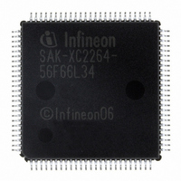
SAK-XC2264-56F66L AC Infineon Technologies, SAK-XC2264-56F66L AC Datasheet - Page 31

SAK-XC2264-56F66L AC
Manufacturer Part Number
SAK-XC2264-56F66L AC
Description
IC MCU 16BIT FLASH PG-LQFP-100
Manufacturer
Infineon Technologies
Series
XC22xxr
Datasheet
1.SAK-XC2264-56F66L_AC.pdf
(116 pages)
Specifications of SAK-XC2264-56F66L AC
Core Processor
C166SV2
Core Size
16/32-Bit
Speed
66MHz
Connectivity
CAN, EBI/EMI, I²C, LIN, SPI, SSC, UART/USART, USI
Peripherals
DMA, I²S, POR, PWM, WDT
Number Of I /o
75
Program Memory Size
448KB (448K x 8)
Program Memory Type
FLASH
Ram Size
34K x 8
Voltage - Supply (vcc/vdd)
3 V ~ 5.5 V
Data Converters
A/D 8x8/10b
Oscillator Type
Internal
Operating Temperature
-40°C ~ 125°C
Package / Case
100-LFQFP
Lead Free Status / RoHS Status
Lead free / RoHS Compliant
Eeprom Size
-
Other names
KX226456F66L34ACXT
SAK-XC2264-56F66L34 AC
SAK-XC2264-56F66L34ACINTR
SAK-XC2264-56F66L34ACINTR
SAK-XC2264-56F66LACINTR
SP000300114
SAK-XC2264-56F66L34 AC
SAK-XC2264-56F66L34ACINTR
SAK-XC2264-56F66L34ACINTR
SAK-XC2264-56F66LACINTR
SP000300114
Table 4
Pin
99
10
38,
64,
88
14
2,
25,
27,
50,
52,
75,
77,
100
1,
26,
51,
76
1) To generate the reference clock output for bus timing measurement,
Data Sheet
EXTCLK and P2.8 must be selected as output pin. Also the high-speed clock pad must be enabled. This
configuration is referred to as reference clock output signal CLKOUT.
Symbol
ESR0
U1C0_DX0E
U1C0_DX2B
V
V
V
V
V
DDIM
DDI1
DDPA
DDPB
SS
Pin Definitions and Functions (cont’d)
Ctrl.
O0 / I St/B
I
I
-
-
-
-
-
Type Function
St/B
St/B
PS/M Digital Core Supply Voltage for Domain M
PS/1 Digital Core Supply Voltage for Domain 1
PS/A Digital Pad Supply Voltage for Domain A
PS/B Digital Pad Supply Voltage for Domain B
PS/-- Digital Ground
External Service Request 0
Note: After power-up, ESR0 operates as open-
USIC1 Channel 0 Shift Data Input
USIC1 Channel 0 Shift Control Input
Decouple with a ceramic capacitor, see
for details.
Decouple with a ceramic capacitor, see
for details.
All
Connect decoupling capacitors to adjacent
V
Note: The A/D_Converters and ports P5, P6, and
Connect decoupling capacitors to adjacent
V
Note: The on-chip voltage regulators and all ports
All
or ground-plane.
Note: Also the exposed pad is connected to
DDP
DDP
V
V
DDI1
SS
/
/
V
V
29
drain bidirectional reset with a weak pull-up.
P15 are fed from supply voltage
except P5, P6, and P15 are fed from supply
voltage
The respective board area must be
connected to ground (if soldered) or left free.
SS
SS
pins must be connected to the ground-line
pins must be connected to each other.
pin pairs as close as possible to the pins.
pin pairs as close as possible to the pins.
V
DDPB
XC2000 Family Derivatives
.
General Device Information
f
SYS
must be selected as source for
XC2267 / XC2264
V2.1, 2008-08
V
Table 12
Table 12
DDPA
.
V
SS
.


