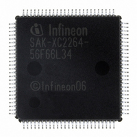
SAK-XC2264-56F66L AC Infineon Technologies, SAK-XC2264-56F66L AC Datasheet - Page 12

SAK-XC2264-56F66L AC
Manufacturer Part Number
SAK-XC2264-56F66L AC
Description
IC MCU 16BIT FLASH PG-LQFP-100
Manufacturer
Infineon Technologies
Series
XC22xxr
Datasheet
1.SAK-XC2264-56F66L_AC.pdf
(116 pages)
Specifications of SAK-XC2264-56F66L AC
Core Processor
C166SV2
Core Size
16/32-Bit
Speed
66MHz
Connectivity
CAN, EBI/EMI, I²C, LIN, SPI, SSC, UART/USART, USI
Peripherals
DMA, I²S, POR, PWM, WDT
Number Of I /o
75
Program Memory Size
448KB (448K x 8)
Program Memory Type
FLASH
Ram Size
34K x 8
Voltage - Supply (vcc/vdd)
3 V ~ 5.5 V
Data Converters
A/D 8x8/10b
Oscillator Type
Internal
Operating Temperature
-40°C ~ 125°C
Package / Case
100-LFQFP
Lead Free Status / RoHS Status
Lead free / RoHS Compliant
Eeprom Size
-
Other names
KX226456F66L34ACXT
SAK-XC2264-56F66L34 AC
SAK-XC2264-56F66L34ACINTR
SAK-XC2264-56F66L34ACINTR
SAK-XC2264-56F66LACINTR
SP000300114
SAK-XC2264-56F66L34 AC
SAK-XC2264-56F66L34ACINTR
SAK-XC2264-56F66L34ACINTR
SAK-XC2264-56F66LACINTR
SP000300114
- Current page: 12 of 116
- Download datasheet (2Mb)
Notes to Pin Definitions
1. Ctrl.: The output signal for a port pin is selected by bitfield PC in the associated
2. Type: Indicates the pad type used (St=standard pad, Sp=special pad, DP=double
Table 4
Pin
3
4
5
6
Data Sheet
register Px_IOCRy. Output O0 is selected by setting the respective bitfield PC to
1x00
Output signal OH is controlled by hardware.
pad, In=input pad, PS=power supply) and its power supply domain (A, B, M, 1).
Symbol
TESTM
P7.2
EMUX0
TxDC4
CCU62_
CCPOS0A
TDI_C
TRST
P7.0
T3OUT
T6OUT
TDO_A
ESR2_1
RxDC4B
B
, output O1 is selected by 1x01
Pin Definitions and Functions
Ctrl.
I
O0 / I St/B
O1
O2
I
I
I
O0 / I St/B
O1
O2
OH
I
I
Type Function
In/B
St/B
St/B
St/B
St/B
In/B
St/B
St/B
St/B
St/B
St/B
Testmode Enable
Enables factory test modes, must be held HIGH for
normal operation (connect to
An internal pullup device will hold this pin high
when nothing is driving it.
Bit 2 of Port 7, General Purpose Input/Output
External Analog MUX Control Output 0 (ADC1)
CAN Node 4 Transmit Data Output
CCU62 Position Input 0
JTAG Test Data Input
Test-System Reset Input
For normal system operation, pin TRST should be
held low. A high level at this pin at the rising edge
of PORST activates the XC226x’s debug system.
In this case, pin TRST must be driven low once to
reset the debug system.
An internal pulldown device will hold this pin low
when nothing is driving it.
Bit 0 of Port 7, General Purpose Input/Output
GPT1 Timer T3 Toggle Latch Output
GPT2 Timer T6 Toggle Latch Output
JTAG Test Data Output
ESR2 Trigger Input 1
CAN Node 4 Receive Data Input
B
, etc.
10
XC2000 Family Derivatives
General Device Information
V
XC2267 / XC2264
DDPB
).
V2.1, 2008-08
Related parts for SAK-XC2264-56F66L AC
Image
Part Number
Description
Manufacturer
Datasheet
Request
R

Part Number:
Description:
Microcontrollers (MCU) 16 BIT FLASH C11 BCS
Manufacturer:
Infineon Technologies

Part Number:
Description:
16/32-Bit Single-Chip Microcontroller with 32-Bit Performance
Manufacturer:
INFINEON [Infineon Technologies AG]
Datasheet:

Part Number:
Description:
Manufacturer:
Infineon Technologies AG
Datasheet:

Part Number:
Description:
Manufacturer:
Infineon Technologies AG
Datasheet:

Part Number:
Description:
Manufacturer:
Infineon Technologies AG
Datasheet:

Part Number:
Description:
Manufacturer:
Infineon Technologies AG
Datasheet:

Part Number:
Description:
Manufacturer:
Infineon Technologies AG
Datasheet:

Part Number:
Description:
Manufacturer:
Infineon Technologies AG
Datasheet:

Part Number:
Description:
Manufacturer:
Infineon Technologies AG
Datasheet:

Part Number:
Description:
16-bit microcontroller with 2x2 KByte RAM
Manufacturer:
Infineon Technologies AG
Datasheet:

Part Number:
Description:
NPN silicon RF transistor
Manufacturer:
Infineon Technologies AG
Datasheet:

Part Number:
Description:
NPN silicon RF transistor
Manufacturer:
Infineon Technologies AG
Datasheet:

Part Number:
Description:
NPN silicon RF transistor
Manufacturer:
Infineon Technologies AG
Datasheet:

Part Number:
Description:
NPN silicon RF transistor
Manufacturer:
Infineon Technologies AG
Datasheet:

Part Number:
Description:
Si-MMIC-amplifier in SIEGET 25-technologie
Manufacturer:
Infineon Technologies AG
Datasheet:


