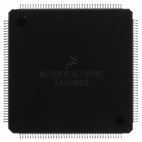
MC56F8367VPYE Freescale Semiconductor, MC56F8367VPYE Datasheet - Page 47

MC56F8367VPYE
Manufacturer Part Number
MC56F8367VPYE
Description
IC DSP 16BIT 60MHZ 160-LQFP
Manufacturer
Freescale Semiconductor
Series
56F8xxxr
Specifications of MC56F8367VPYE
Core Processor
56800
Core Size
16-Bit
Speed
60MHz
Connectivity
CAN, EBI/EMI, SCI, SPI
Peripherals
POR, PWM, Temp Sensor, WDT
Number Of I /o
76
Program Memory Size
544KB (272K x 16)
Program Memory Type
FLASH
Ram Size
18K x 16
Voltage - Supply (vcc/vdd)
2.25 V ~ 3.6 V
Data Converters
A/D 16x12b
Oscillator Type
External
Operating Temperature
-40°C ~ 105°C
Package / Case
160-LQFP
Cpu Family
56F8xxx
Device Core Size
16b
Frequency (max)
60MHz
Interface Type
CAN/SCI/SPI
Total Internal Ram Size
36KB
# I/os (max)
76
Number Of Timers - General Purpose
4
Operating Supply Voltage (typ)
3.3V
Operating Supply Voltage (max)
3.6V
Operating Supply Voltage (min)
3V
On-chip Adc
4(4-chx12-bit)
Instruction Set Architecture
CISC
Operating Temp Range
-40C to 105C
Operating Temperature Classification
Industrial
Mounting
Surface Mount
Pin Count
160
Package Type
LQFP
Data Bus Width
16 bit
Processor Series
MC56F83xx
Core
56800E
Numeric And Arithmetic Format
Fixed-Point
Device Million Instructions Per Second
60 MIPs
Maximum Clock Frequency
60 MHz
Number Of Programmable I/os
76
Data Ram Size
36 KB
Operating Supply Voltage
3.3 V
Maximum Operating Temperature
+ 105 C
Mounting Style
SMD/SMT
Development Tools By Supplier
MC56F8367EVME
Minimum Operating Temperature
- 40 C
Package
160LQFP
Family Name
56F8xxx
Maximum Speed
60 MHz
Number Of Timers
4
For Use With
MC56F8367EVME - EVAL BOARD FOR MC56F83X
Lead Free Status / RoHS Status
Lead free / RoHS Compliant
Eeprom Size
-
Lead Free Status / Rohs Status
Compliant
Available stocks
Company
Part Number
Manufacturer
Quantity
Price
Company:
Part Number:
MC56F8367VPYE
Manufacturer:
AM
Quantity:
90
Company:
Part Number:
MC56F8367VPYE
Manufacturer:
Freescale Semiconductor
Quantity:
10 000
Part Number:
MC56F8367VPYE
Manufacturer:
FREESCALE
Quantity:
20 000
4.4 Data Map
Note: Data Flash is NOT available on the 56F8167 device.
4.5 Flash Memory Map
Figure 4-1
The Flash Memory is divided into three functional blocks. The Program and boot memories reside on the
Program Memory buses. They are controlled by one set of banked registers. Data Memory Flash resides
on the Data Memory buses and is controlled separately by its own set of banked registers.
The top nine words of the Program Memory Flash are treated as special memory locations. The content of
these words is used to control the operation of the Flash Controller. Because these words are part of the
Flash Memory content, their state is maintained during power down and reset. During chip initialization,
the content of these memory locations is loaded into Flash Memory control registers, detailed in the Flash
Memory chapter of the 56F8300 Peripheral User Manual. These configuration parameters are located
between $03_FFF7 and $03_FFFF.
Freescale Semiconductor
Preliminary
1. All addresses are 16-bit Word addresses, not byte addresses.
2. In the Operating Mode Register (OMR).
3. The Data RAM is organized as an 8K x 32-bit memory to allow single-cycle, long-word operations.
X:$FF FFFF
X:$FF FF00
X:$FF FEFF
X:$01 0000
X:$00 FFFF
X:$00 F000
X:$00 EFFF
X:$00 8000
X:$00 7FFF
X:$00 4000
X:$00 3FFF
X:$00 0000
Begin/End
Address
illustrates the Flash Memory (FM) map on the system bus.
EOnCE
256 locations allocated
External Memory
On-Chip Peripherals
4096 locations allocated
External Memory
On-Chip Data Flash
32KB
On-Chip Data RAM
32KB
3
Table 4-6 Data Memory Map
EX = 0
56F8367 Technical Data, Rev. 8
2
EOnCE
256 locations allocated
External Memory
On-Chip Peripherals
4096 locations allocated
External Memory
1
EX = 1
Data Map
47


