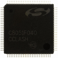
C8051F040-GQ Silicon Laboratories Inc, C8051F040-GQ Datasheet - Page 207

C8051F040-GQ
Manufacturer Part Number
C8051F040-GQ
Description
IC 8051 MCU 64K FLASH 100TQFP
Manufacturer
Silicon Laboratories Inc
Series
C8051F04xr
Datasheets
1.C8051F040-TB.pdf
(328 pages)
2.C8051F040-TB.pdf
(2 pages)
3.C8051F043-GQ.pdf
(328 pages)
Specifications of C8051F040-GQ
Program Memory Type
FLASH
Program Memory Size
64KB (64K x 8)
Package / Case
100-TQFP, 100-VQFP
Core Processor
8051
Core Size
8-Bit
Speed
25MHz
Connectivity
CAN, EBI/EMI, SMBus (2-Wire/I²C), SPI, UART/USART
Peripherals
Brown-out Detect/Reset, POR, PWM, Temp Sensor, WDT
Number Of I /o
64
Ram Size
4.25K x 8
Voltage - Supply (vcc/vdd)
2.7 V ~ 3.6 V
Data Converters
A/D 8x8b, 13x12b; D/A 2x10b, 2x12b
Oscillator Type
Internal
Operating Temperature
-40°C ~ 85°C
Processor Series
C8051F0x
Core
8051
Data Bus Width
8 bit
Data Ram Size
4.25 KB
Interface Type
CAN/SMBus/SPI/UART
Maximum Clock Frequency
25 MHz
Number Of Programmable I/os
64
Number Of Timers
5
Operating Supply Voltage
2.7 V to 3.6 V
Maximum Operating Temperature
+ 85 C
Mounting Style
SMD/SMT
3rd Party Development Tools
PK51, CA51, A51, ULINK2
Development Tools By Supplier
C8051F040DK
Minimum Operating Temperature
- 40 C
On-chip Adc
8-ch x 8-bit or 13-ch x 12-bit
On-chip Dac
2-ch x 12-bit
No. Of I/o's
64
Ram Memory Size
4352Byte
Cpu Speed
25MHz
No. Of Timers
5
Rohs Compliant
Yes
Data Rom Size
64 KB
A/d Bit Size
12 bit
A/d Channels Available
13
Height
1 mm
Length
14 mm
Supply Voltage (max)
3.6 V
Supply Voltage (min)
2.7 V
Width
14 mm
Package
100TQFP
Device Core
8051
Family Name
C8051F04x
Maximum Speed
25 MHz
Lead Free Status / RoHS Status
Lead free / RoHS Compliant
For Use With
336-1205 - DEV KIT FOR F040/F041/F042/F043
Eeprom Size
-
Lead Free Status / Rohs Status
Lead free / RoHS Compliant
Other names
336-1204
Available stocks
Company
Part Number
Manufacturer
Quantity
Price
Company:
Part Number:
C8051F040-GQ
Manufacturer:
SiliconL
Quantity:
702
Company:
Part Number:
C8051F040-GQ
Manufacturer:
Silicon Laboratories Inc
Quantity:
10 000
Company:
Part Number:
C8051F040-GQR
Manufacturer:
Silicon Laboratories Inc
Quantity:
10 000
Part Number:
C8051F040-GQR
Manufacturer:
SILICON LABS/芯科
Quantity:
20 000
a digital input by setting P3MDOUT.7 to a logic 0, which selects open-drain output mode, and P3.7 to a
logic 1, which disables the low-side output driver.
If the Port pin has been assigned to a digital peripheral by the Crossbar and that pin functions as an input
(for example RX0, the UART0 receive pin), then the output drivers on that pin are automatically disabled.
17.1.4. Weak Pullups
By default, each Port pin has an internal weak pullup device enabled which provides a resistive connection
(about 100 k) between the pin and V
logic 1 to the Weak Pullup Disable bit, (WEAKPUD, XBR2.7). The weak pullup is automatically deactivated
on any pin that is driving a logic 0; that is, an output pin will not contend with its own pullup device. The
weak pullup device can also be explicitly disabled on Ports 1, 2, and 3 pin by configuring the pin as an
Analog Input, as described below.
17.1.5. Configuring Port 1, 2, and 3 Pins as Analog Inputs
The pins on Port 1 can serve as analog inputs to the ADC2 analog MUX (C8051F040/1/2/3 only), the pins
on Port 2 can serve as analog inputs to the Comparators, and the pins on Port 3 can serve as inputs to
ADC0. A Port pin is configured as an Analog Input by writing a logic 0 to the associated bit in the PnMDIN
registers. All Port pins default to a Digital Input mode. Configuring a Port pin as an analog input:
Note that the output drivers on a pin configured as an Analog Input are not explicitly disabled. Therefore,
the associated PnMDOUT bits of pins configured as Analog Inputs should explicitly be set to logic 0
(Open-Drain output mode), and the associated Port Data bits should be set to logic 1 (high-impedance).
Also note that it is not required to configure a Port pin as an Analog Input in order to use it as an input to
the ADC’s or Comparators; however, it is strongly recommended. See the analog peripheral’s correspond-
ing section in this datasheet for further information.
1. Disables the digital input path from the pin. This prevents additional power supply current from
2. Disables the weak pullup device on the pin.
3. Causes the Crossbar to “skip over” the pin when allocating Port pins for digital peripherals.
being drawn when the voltage at the pin is near V
a logic 0 regardless of the voltage at the Port pin.
DD
. The weak pullup devices can be globally disabled by writing a
Rev. 1.5
C8051F040/1/2/3/4/5/6/7
DD
/ 2. A read of the Port Data bit will return
207


