MC9S12C32CFAE25 Freescale Semiconductor, MC9S12C32CFAE25 Datasheet - Page 386
MC9S12C32CFAE25
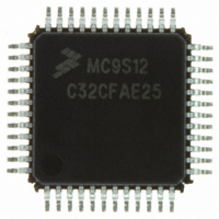
Manufacturer Part Number
MC9S12C32CFAE25
Description
IC MCU 32K FLASH 25MHZ 48-LQFP
Manufacturer
Freescale Semiconductor
Series
HCS12r
Datasheets
1.MC9S12GC16MFUE.pdf
(690 pages)
2.MC9S12C96CFUER.pdf
(26 pages)
3.MC9S12C32CFAE25.pdf
(2 pages)
4.MC9S12C32CPBE25.pdf
(36 pages)
Specifications of MC9S12C32CFAE25
Core Processor
HCS12
Core Size
16-Bit
Speed
25MHz
Connectivity
CAN, EBI/EMI, SCI, SPI
Peripherals
POR, PWM, WDT
Number Of I /o
31
Program Memory Size
32KB (32K x 8)
Program Memory Type
FLASH
Ram Size
2K x 8
Voltage - Supply (vcc/vdd)
2.35 V ~ 5.5 V
Data Converters
A/D 8x10b
Oscillator Type
Internal
Operating Temperature
-40°C ~ 85°C
Package / Case
48-LQFP
Processor Series
S12C
Core
HCS12
Data Bus Width
16 bit
Data Ram Size
2 KB
Interface Type
CAN/SCI/SPI
Maximum Clock Frequency
25 MHz
Number Of Programmable I/os
31
Number Of Timers
8
Maximum Operating Temperature
+ 85 C
Mounting Style
SMD/SMT
3rd Party Development Tools
EWHCS12
Development Tools By Supplier
M68EVB912C32EE
Minimum Operating Temperature
- 40 C
On-chip Adc
8-ch x 10-bit
For Use With
CML12C32SLK - KIT STUDENT LEARNING 16BIT HCS12
Lead Free Status / RoHS Status
Lead free / RoHS Compliant
Eeprom Size
-
Lead Free Status / Rohs Status
Lead free / RoHS Compliant
Available stocks
Company
Part Number
Manufacturer
Quantity
Price
Company:

Part Number:
MC9S12C32CFAE25
Manufacturer:
FREESCAL
Quantity:
240
Company:
Part Number:
MC9S12C32CFAE25
Manufacturer:
Freescale Semiconductor
Quantity:
10 000


Chapter 13 Serial Communications Interface (S12SCIV2) Block Description
13.3
This section provides a detailed description of all memory and registers.
13.3.1
The memory map for the SCI module is given below in
is the address offset. The total address for each register is the sum of the base address for the SCI module
and the address offset for each register.
13.3.2
This section consists of register descriptions in address order. Each description includes a standard register
diagram with an associated figure number. Writes to a reserved register location do not have any effect and
reads of these locations return a zero. Details of register bit and field function follow the register diagrams,
in bit order.
386
Address
0x0000
0x0001
0x0002
0x0003
0x0004
0x0005
0x0006
0x0007
Memory Map and Registers
Module Memory Map
Register Descriptions
SCIDRH
SCIBDH
SCIBDL
SCICR1
SCICR2
SCISR1
SCISR2
SCIDRL
Name
W
W
W
W
W
W
W
W
R
R
R
R
R
R
R
R
LOOPS
TDRE
SBR7
Bit 7
TIE
R8
R7
T7
0
0
Figure 13-2. SCI Register Summary
MC9S12C-Family / MC9S12GC-Family
= Unimplemented or Reserved
SCISWAI
SBR6
TCIE
TC
R6
T8
T6
6
0
0
Rev 01.24
RSRC
RDRF
SBR5
RIE
R5
T5
5
0
0
0
Figure
SBR12
SBR4
IDLE
ILIE
R4
T4
M
4
0
0
13-2. The Address listed for each register
SBR11
WAKE
SBR3
OR
TE
R3
T3
3
0
0
SBR10
BRK13
SBR2
ILT
RE
NF
R2
T2
2
0
Freescale Semiconductor
TXDIR
SBR9
SBR1
RWU
PE
FE
R1
T1
1
0
SBR8
SBR0
Bit 0
SBK
RAF
PT
PF
R0
T0
0
Related parts for MC9S12C32CFAE25
Image
Part Number
Description
Manufacturer
Datasheet
Request
R

Part Number:
Description:
Manufacturer:
Freescale Semiconductor, Inc
Datasheet:
Part Number:
Description:
Manufacturer:
Freescale Semiconductor, Inc
Datasheet:
Part Number:
Description:
Manufacturer:
Freescale Semiconductor, Inc
Datasheet:
Part Number:
Description:
Manufacturer:
Freescale Semiconductor, Inc
Datasheet:
Part Number:
Description:
Manufacturer:
Freescale Semiconductor, Inc
Datasheet:
Part Number:
Description:
Manufacturer:
Freescale Semiconductor, Inc
Datasheet:
Part Number:
Description:
Manufacturer:
Freescale Semiconductor, Inc
Datasheet:
Part Number:
Description:
Manufacturer:
Freescale Semiconductor, Inc
Datasheet:
Part Number:
Description:
Manufacturer:
Freescale Semiconductor, Inc
Datasheet:
Part Number:
Description:
Manufacturer:
Freescale Semiconductor, Inc
Datasheet:
Part Number:
Description:
Manufacturer:
Freescale Semiconductor, Inc
Datasheet:
Part Number:
Description:
Manufacturer:
Freescale Semiconductor, Inc
Datasheet:
Part Number:
Description:
Manufacturer:
Freescale Semiconductor, Inc
Datasheet:
Part Number:
Description:
Manufacturer:
Freescale Semiconductor, Inc
Datasheet:
Part Number:
Description:
Manufacturer:
Freescale Semiconductor, Inc
Datasheet: