MC908SR12MFAE Freescale Semiconductor, MC908SR12MFAE Datasheet - Page 234
MC908SR12MFAE
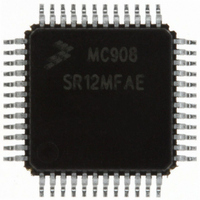
Manufacturer Part Number
MC908SR12MFAE
Description
IC MCU 12K FLASH 8MHZ 48-LQFP
Manufacturer
Freescale Semiconductor
Series
HC08r
Datasheet
1.MC908SR12MFAE.pdf
(404 pages)
Specifications of MC908SR12MFAE
Core Processor
HC08
Core Size
8-Bit
Speed
8MHz
Connectivity
I²C, SCI
Peripherals
LVD, POR, PWM, Temp Sensor
Number Of I /o
31
Program Memory Size
12KB (12K x 8)
Program Memory Type
FLASH
Ram Size
512 x 8
Voltage - Supply (vcc/vdd)
4.5 V ~ 5.5 V
Data Converters
A/D 14x10b
Oscillator Type
Internal
Operating Temperature
-40°C ~ 125°C
Package / Case
48-LQFP
Lead Free Status / RoHS Status
Lead free / RoHS Compliant
Eeprom Size
-
Available stocks
Company
Part Number
Manufacturer
Quantity
Price
Company:

Part Number:
MC908SR12MFAE
Manufacturer:
Freescale Semiconductor
Quantity:
10 000
Company:
Part Number:
MC908SR12MFAER
Manufacturer:
Freescale Semiconductor
Quantity:
10 000


Analog-to-Digital Converter (ADC)
15.4 Functional Description
15.4.1 ADC Port I/O Pins
Data Sheet
234
The ADC provides thirteen pins for sampling external sources at pins
PTA0/ATD2–PTA5/ATD7, PTC3/ATD8–PTC7/ATD12, and
OPIN1–OPIN2; one internal source from the analog module. An analog
multiplexer allows the single ADC converter to select one of fourteen
ADC channels as ADC voltage in (V
successive approximation register-based analog-to-digital converter.
When the conversion is completed, ADC places the result in the ADC
data register, high and low byte (ADRH0 and ADRL0), and sets a flag or
generates an interrupt.
An additional three ADC data registers (ADRL1–ADRL3) are available to
store the individual converted data for ADC channels ATD1–ATD3 when
the auto-scan mode is enabled. Data from channel ATD0 is stored in
ADRL0 in the auto-scan mode.
Figure 15-2
PTA0–PTA5 and PTC3–PTC7 are general-purpose I/O pins that are
shared with the ADC channels, OPIN1 and OPIN2 are two analog inputs
that are always connected to the ADC channel select multiplexer. The
channel select bits, ADCH[4:0], define which ADC channel/port pin will
be used as the input signal. The ADC overrides the port I/O logic by
forcing that pin as input to the ADC. The remaining ADC channels/port
pins are controlled by the port I/O logic and can be used as general-
purpose I/O pins. Writes to the port data register or data direction
register will not have any affect on the port pin that is selected by the
ADC. Read of a port pin which is in use by the ADC will return the pin
condition if the corresponding DDR bit is at logic 0. If the DDR bit is at
logic 1, the value in the port data latch is read.
Analog-to-Digital Converter (ADC)
shows the structure of the ADC module.
MC68HC908SR12•MC68HC08SR12 — Rev. 5.0
ADIN
). V
ADIN
is converted by the
Freescale Semiconductor
Related parts for MC908SR12MFAE
Image
Part Number
Description
Manufacturer
Datasheet
Request
R

Part Number:
Description:
Manufacturer:
Freescale Semiconductor, Inc
Datasheet:
Part Number:
Description:
Manufacturer:
Freescale Semiconductor, Inc
Datasheet:
Part Number:
Description:
Manufacturer:
Freescale Semiconductor, Inc
Datasheet:
Part Number:
Description:
Manufacturer:
Freescale Semiconductor, Inc
Datasheet:
Part Number:
Description:
Manufacturer:
Freescale Semiconductor, Inc
Datasheet:
Part Number:
Description:
Manufacturer:
Freescale Semiconductor, Inc
Datasheet:
Part Number:
Description:
Manufacturer:
Freescale Semiconductor, Inc
Datasheet:
Part Number:
Description:
Manufacturer:
Freescale Semiconductor, Inc
Datasheet:
Part Number:
Description:
Manufacturer:
Freescale Semiconductor, Inc
Datasheet:
Part Number:
Description:
Manufacturer:
Freescale Semiconductor, Inc
Datasheet:
Part Number:
Description:
Manufacturer:
Freescale Semiconductor, Inc
Datasheet:
Part Number:
Description:
Manufacturer:
Freescale Semiconductor, Inc
Datasheet:
Part Number:
Description:
Manufacturer:
Freescale Semiconductor, Inc
Datasheet:
Part Number:
Description:
Manufacturer:
Freescale Semiconductor, Inc
Datasheet:
Part Number:
Description:
Manufacturer:
Freescale Semiconductor, Inc
Datasheet: