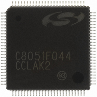
C8051F044-GQ Silicon Laboratories Inc, C8051F044-GQ Datasheet - Page 297

C8051F044-GQ
Manufacturer Part Number
C8051F044-GQ
Description
IC 8051 MCU 64K FLASH 100TQFP
Manufacturer
Silicon Laboratories Inc
Series
C8051F04xr
Specifications of C8051F044-GQ
Program Memory Type
FLASH
Program Memory Size
64KB (64K x 8)
Package / Case
100-TQFP, 100-VQFP
Core Processor
8051
Core Size
8-Bit
Speed
25MHz
Connectivity
CAN, EBI/EMI, SMBus (2-Wire/I²C), SPI, UART/USART
Peripherals
Brown-out Detect/Reset, POR, PWM, Temp Sensor, WDT
Number Of I /o
64
Ram Size
4.25K x 8
Voltage - Supply (vcc/vdd)
2.7 V ~ 3.6 V
Data Converters
A/D 13x10b
Oscillator Type
Internal
Operating Temperature
-40°C ~ 85°C
Processor Series
C8051F0x
Core
8051
Data Bus Width
8 bit
Data Ram Size
4.25 KB
Interface Type
CAN/SMBus/SPI/UART
Maximum Clock Frequency
25 MHz
Number Of Programmable I/os
64
Number Of Timers
5
Operating Supply Voltage
2.7 V to 3.6 V
Maximum Operating Temperature
+ 85 C
Mounting Style
SMD/SMT
3rd Party Development Tools
PK51, CA51, A51, ULINK2
Development Tools By Supplier
C8051F040DK
Minimum Operating Temperature
- 40 C
On-chip Adc
13-ch x 10-bit
On-chip Dac
2-ch x 12-bit
No. Of I/o's
64
Ram Memory Size
4352Byte
Cpu Speed
25MHz
No. Of Timers
5
Rohs Compliant
Yes
Package
100TQFP
Device Core
8051
Family Name
C8051F04x
Maximum Speed
25 MHz
Data Rom Size
64 KB
A/d Bit Size
10 bit
A/d Channels Available
13
Height
1 mm
Length
14 mm
Supply Voltage (max)
3.6 V
Supply Voltage (min)
2.7 V
Width
14 mm
Lead Free Status / RoHS Status
Lead free / RoHS Compliant
Eeprom Size
-
Lead Free Status / Rohs Status
Lead free / RoHS Compliant
Other names
336-1209
Available stocks
Company
Part Number
Manufacturer
Quantity
Price
Company:
Part Number:
C8051F044-GQ
Manufacturer:
AMD
Quantity:
883
Company:
Part Number:
C8051F044-GQ
Manufacturer:
SiliconL
Quantity:
3 169
Company:
Part Number:
C8051F044-GQ
Manufacturer:
Silicon Laboratories Inc
Quantity:
10 000
Company:
Part Number:
C8051F044-GQR
Manufacturer:
Silicon Laboratories Inc
Quantity:
10 000
C8051F040/1/2/3/4/5/6/7
23.2. Timer 2, Timer 3, and Timer 4
Timers n are 16-bit counter/timers, each formed by two 8-bit SFRs: TMRnL (low byte) and TMRnH (high
byte) where n = 2, 3, and 4 for timers 2, 3, and 4 respectively. These timers feature auto-reload, capture,
and toggle output modes with the ability to count up or down. Capture Mode and Auto-reload mode are
selected using bits in the Timer n Control registers (TMRnCN). Toggle output mode is selected using the
Timer 2, 3, and 4 Configuration registers (TMRnCF). These timers may also be used to generate a square-
wave at an external pin. As with Timers 0 and 1, Timers n can use either the system clock (divided by one,
two, or twelve), external clock (divided by eight) or transitions on an external input pin as its clock source.
The Counter/Timer Select bit C/Tn (TMRnCN.1) configures the peripheral as a counter or timer. Clearing
C/Tn configures the Timer to be in a timer mode (i.e., the system clock or external clock as input for the
timer). When C/Tn is set to 1, the timer is configured as a counter (i.e., high-to-low transitions at the Tn
input pin increment (or decrement) the counter/timer register). Refer to
Section “17.1. Ports 0 through 3
and the Priority Crossbar Decoder” on page 204
for information on selecting and configuring external I/
O pins for digital peripherals, such as the Tn pin. Timer 2 and 3 can be used to start an ADC Data Conver-
sion and Timers 2, 3, and 4 can schedule DAC outputs. Only Timer 1 can be used to generate baud rates
for UART 1, and Timers 1, 2, 3, or 4 may be used to generate baud rates for UART 0.
Timer n can use either SYSCLK, SYSCLK divided by 2, SYSCLK divided by 12, an external clock divided
by 8, or high-to-low transitions on the Tn input pin as its clock source when operating in Counter/Timer with
Capture mode. Clearing the C/Tn bit (TMRnCN.1) selects the system clock/external clock as the input for
the timer. The Timer Clock Select bits TnM0 and TnM1 in TMRnCF can be used to select the system clock
undivided, system clock divided by two, system clock divided by 12, or an external clock provided at the
XTAL1/XTAL2 pins divided by 8 (see SFR Definition 23.9). When C/Tn is set to logic 1, a high-to-low tran-
sition at the Tn input pin increments the counter/timer register (i.e., configured as a counter).
23.2.1. Configuring Timer 2, 3, and 4 to Count Down
Timers 2, 3, and 4 have the ability to count down. When the timer’s respective Decrement Enable Bit
(DCEN) in the Timer Configuration Register (See SFR Definition 23.9) is set to ‘1’, the timer can then count
up or down. When DCEN = 1, the direction of the timer’s count is controlled by the TnEX pin’s logic level.
When TnEX = 1, the counter/timer will count up; when TnEX = 0, the counter/timer will count down. To use
this feature, TnEX must be enabled in the digital crossbar and configured as a digital input.
Note: When DCEN = 1, other functions of the TnEX input (i.e., capture and auto-reload) are not available.
TnEX will only control the direction of the timer when DCEN = 1.
Rev. 1.5
295


