C8051F044-GQ Silicon Laboratories Inc, C8051F044-GQ Datasheet - Page 11
C8051F044-GQ
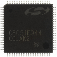
Manufacturer Part Number
C8051F044-GQ
Description
IC 8051 MCU 64K FLASH 100TQFP
Manufacturer
Silicon Laboratories Inc
Series
C8051F04xr
Specifications of C8051F044-GQ
Program Memory Type
FLASH
Program Memory Size
64KB (64K x 8)
Package / Case
100-TQFP, 100-VQFP
Core Processor
8051
Core Size
8-Bit
Speed
25MHz
Connectivity
CAN, EBI/EMI, SMBus (2-Wire/I²C), SPI, UART/USART
Peripherals
Brown-out Detect/Reset, POR, PWM, Temp Sensor, WDT
Number Of I /o
64
Ram Size
4.25K x 8
Voltage - Supply (vcc/vdd)
2.7 V ~ 3.6 V
Data Converters
A/D 13x10b
Oscillator Type
Internal
Operating Temperature
-40°C ~ 85°C
Processor Series
C8051F0x
Core
8051
Data Bus Width
8 bit
Data Ram Size
4.25 KB
Interface Type
CAN/SMBus/SPI/UART
Maximum Clock Frequency
25 MHz
Number Of Programmable I/os
64
Number Of Timers
5
Operating Supply Voltage
2.7 V to 3.6 V
Maximum Operating Temperature
+ 85 C
Mounting Style
SMD/SMT
3rd Party Development Tools
PK51, CA51, A51, ULINK2
Development Tools By Supplier
C8051F040DK
Minimum Operating Temperature
- 40 C
On-chip Adc
13-ch x 10-bit
On-chip Dac
2-ch x 12-bit
No. Of I/o's
64
Ram Memory Size
4352Byte
Cpu Speed
25MHz
No. Of Timers
5
Rohs Compliant
Yes
Package
100TQFP
Device Core
8051
Family Name
C8051F04x
Maximum Speed
25 MHz
Data Rom Size
64 KB
A/d Bit Size
10 bit
A/d Channels Available
13
Height
1 mm
Length
14 mm
Supply Voltage (max)
3.6 V
Supply Voltage (min)
2.7 V
Width
14 mm
Lead Free Status / RoHS Status
Lead free / RoHS Compliant
Eeprom Size
-
Lead Free Status / Rohs Status
Lead free / RoHS Compliant
Other names
336-1209
Available stocks
Company
Part Number
Manufacturer
Quantity
Price
Company:

Part Number:
C8051F044-GQ
Manufacturer:
AMD
Quantity:
883
Company:
Part Number:
C8051F044-GQ
Manufacturer:
SiliconL
Quantity:
3 169
Company:
Part Number:
C8051F044-GQ
Manufacturer:
Silicon Laboratories Inc
Quantity:
10 000
Company:
Part Number:
C8051F044-GQR
Manufacturer:
Silicon Laboratories Inc
Quantity:
10 000


16. External Data Memory Interface and On-Chip XRAM
17. Port Input/Output
18. Controller Area Network (CAN0)
19. System Management BUS/I
20. Enhanced Serial Peripheral Interface (SPI0)
21. UART0
Figure 16.1. Multiplexed Configuration Example.................................................... 191
Figure 16.2. Non-multiplexed Configuration Example ............................................ 192
Figure 16.3. EMIF Operating Modes ...................................................................... 193
Figure 16.4. Non-multiplexed 16-bit MOVX Timing ................................................ 196
Figure 16.5. Non-multiplexed 8-bit MOVX without Bank Select Timing ................. 197
Figure 16.6. Non-multiplexed 8-bit MOVX with Bank Select Timing ...................... 198
Figure 16.7. Multiplexed 16-bit MOVX Timing........................................................ 199
Figure 16.8. Multiplexed 8-bit MOVX without Bank Select Timing ......................... 200
Figure 16.9. Multiplexed 8-bit MOVX with Bank Select Timing .............................. 201
Figure 17.1. Port I/O Cell Block Diagram ............................................................... 203
Figure 17.2. Port I/O Functional Block Diagram ..................................................... 204
Figure 17.3. Priority Crossbar Decode Table ......................................................... 205
Figure 17.4. Priority Crossbar Decode Table ......................................................... 208
Figure 17.5. Priority Crossbar Decode Table ......................................................... 209
Figure 17.6. Crossbar Example:............................................................................. 211
Figure 18.1. Typical CAN Bus Configuration.......................................................... 227
Figure 18.2. CAN Controller Diagram..................................................................... 228
Figure 18.3. Four Segments of a CAN Bit Time ..................................................... 229
Figure 18.4. CAN0DATH: CAN Data Access Register High Byte .......................... 234
Figure 19.1. SMBus0 Block Diagram ..................................................................... 239
Figure 19.2. Typical SMBus Configuration ............................................................. 240
Figure 19.3. SMBus Transaction ............................................................................ 241
Figure 19.4. Typical Master Transmitter Sequence................................................ 242
Figure 19.5. Typical Master Receiver Sequence.................................................... 243
Figure 19.6. Typical Slave Transmitter Sequence.................................................. 243
Figure 19.7. Typical Slave Receiver Sequence...................................................... 244
Figure 20.1. SPI Block Diagram ............................................................................. 255
Figure 20.2. Multiple-Master Mode Connection Diagram ....................................... 258
Figure 20.3. 3-Wire Single Master and Slave Mode Connection Diagram ............. 258
Figure 20.4. 4-Wire Single Master and Slave Mode Connection Diagram ............. 258
Figure 20.5. Data/Clock Timing Diagram ............................................................... 260
Figure 21.1. UART0 Block Diagram ....................................................................... 265
Figure 21.2. UART0 Mode 0 Timing Diagram ........................................................ 266
Figure 21.3. UART0 Mode 0 Interconnect.............................................................. 267
Figure 21.4. UART0 Mode 1 Timing Diagram ........................................................ 267
Figure 21.5. UART0 Modes 2 and 3 Timing Diagram ............................................ 269
Figure 21.6. UART0 Modes 1, 2, and 3 Interconnect Diagram .............................. 269
Figure 21.7. UART Multi-Processor Mode Interconnect Diagram .......................... 272
2
C BUS (SMBUS0)
Rev. 1.5
C8051F040/1/2/3/4/5/6/7
11
Related parts for C8051F044-GQ
Image
Part Number
Description
Manufacturer
Datasheet
Request
R

Part Number:
Description:
SMD/C°/SINGLE-ENDED OUTPUT SILICON OSCILLATOR
Manufacturer:
Silicon Laboratories Inc
Part Number:
Description:
Manufacturer:
Silicon Laboratories Inc
Datasheet:
Part Number:
Description:
N/A N/A/SI4010 AES KEYFOB DEMO WITH LCD RX
Manufacturer:
Silicon Laboratories Inc
Datasheet:
Part Number:
Description:
N/A N/A/SI4010 SIMPLIFIED KEY FOB DEMO WITH LED RX
Manufacturer:
Silicon Laboratories Inc
Datasheet:
Part Number:
Description:
N/A/-40 TO 85 OC/EZLINK MODULE; F930/4432 HIGH BAND (REV E/B1)
Manufacturer:
Silicon Laboratories Inc
Part Number:
Description:
EZLink Module; F930/4432 Low Band (rev e/B1)
Manufacturer:
Silicon Laboratories Inc
Part Number:
Description:
I°/4460 10 DBM RADIO TEST CARD 434 MHZ
Manufacturer:
Silicon Laboratories Inc
Part Number:
Description:
I°/4461 14 DBM RADIO TEST CARD 868 MHZ
Manufacturer:
Silicon Laboratories Inc
Part Number:
Description:
I°/4463 20 DBM RFSWITCH RADIO TEST CARD 460 MHZ
Manufacturer:
Silicon Laboratories Inc
Part Number:
Description:
I°/4463 20 DBM RADIO TEST CARD 868 MHZ
Manufacturer:
Silicon Laboratories Inc
Part Number:
Description:
I°/4463 27 DBM RADIO TEST CARD 868 MHZ
Manufacturer:
Silicon Laboratories Inc
Part Number:
Description:
I°/4463 SKYWORKS 30 DBM RADIO TEST CARD 915 MHZ
Manufacturer:
Silicon Laboratories Inc
Part Number:
Description:
N/A N/A/-40 TO 85 OC/4463 RFMD 30 DBM RADIO TEST CARD 915 MHZ
Manufacturer:
Silicon Laboratories Inc
Part Number:
Description:
I°/4463 20 DBM RADIO TEST CARD 169 MHZ
Manufacturer:
Silicon Laboratories Inc