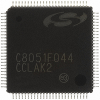
C8051F044-GQ Silicon Laboratories Inc, C8051F044-GQ Datasheet - Page 180

C8051F044-GQ
Manufacturer Part Number
C8051F044-GQ
Description
IC 8051 MCU 64K FLASH 100TQFP
Manufacturer
Silicon Laboratories Inc
Series
C8051F04xr
Specifications of C8051F044-GQ
Program Memory Type
FLASH
Program Memory Size
64KB (64K x 8)
Package / Case
100-TQFP, 100-VQFP
Core Processor
8051
Core Size
8-Bit
Speed
25MHz
Connectivity
CAN, EBI/EMI, SMBus (2-Wire/I²C), SPI, UART/USART
Peripherals
Brown-out Detect/Reset, POR, PWM, Temp Sensor, WDT
Number Of I /o
64
Ram Size
4.25K x 8
Voltage - Supply (vcc/vdd)
2.7 V ~ 3.6 V
Data Converters
A/D 13x10b
Oscillator Type
Internal
Operating Temperature
-40°C ~ 85°C
Processor Series
C8051F0x
Core
8051
Data Bus Width
8 bit
Data Ram Size
4.25 KB
Interface Type
CAN/SMBus/SPI/UART
Maximum Clock Frequency
25 MHz
Number Of Programmable I/os
64
Number Of Timers
5
Operating Supply Voltage
2.7 V to 3.6 V
Maximum Operating Temperature
+ 85 C
Mounting Style
SMD/SMT
3rd Party Development Tools
PK51, CA51, A51, ULINK2
Development Tools By Supplier
C8051F040DK
Minimum Operating Temperature
- 40 C
On-chip Adc
13-ch x 10-bit
On-chip Dac
2-ch x 12-bit
No. Of I/o's
64
Ram Memory Size
4352Byte
Cpu Speed
25MHz
No. Of Timers
5
Rohs Compliant
Yes
Package
100TQFP
Device Core
8051
Family Name
C8051F04x
Maximum Speed
25 MHz
Data Rom Size
64 KB
A/d Bit Size
10 bit
A/d Channels Available
13
Height
1 mm
Length
14 mm
Supply Voltage (max)
3.6 V
Supply Voltage (min)
2.7 V
Width
14 mm
Lead Free Status / RoHS Status
Lead free / RoHS Compliant
Eeprom Size
-
Lead Free Status / Rohs Status
Lead free / RoHS Compliant
Other names
336-1209
Available stocks
Company
Part Number
Manufacturer
Quantity
Price
Company:
Part Number:
C8051F044-GQ
Manufacturer:
AMD
Quantity:
883
Company:
Part Number:
C8051F044-GQ
Manufacturer:
SiliconL
Quantity:
3 169
Company:
Part Number:
C8051F044-GQ
Manufacturer:
Silicon Laboratories Inc
Quantity:
10 000
Company:
Part Number:
C8051F044-GQR
Manufacturer:
Silicon Laboratories Inc
Quantity:
10 000
C8051F040/1/2/3/4/5/6/7
3/4/5) and all locations above 0x8000 (C8051F046/7) are reserved. Flash writes and erases targeting the
reserved area should be avoided.
Table 15.1. Flash Electrical Characteristics
V
15.2. Non-volatile Data Storage
The Flash memory can be used for non-volatile data storage as well as program code. This allows data
such as calibration coefficients to be calculated and stored at run time. Data is written using the MOVX
write instruction (as described in the previous section) and read using the MOVC instruction.
An additional 128-byte sector of Flash memory is included for non-volatile data storage. Its smaller sector
size makes it particularly well suited as general purpose, non-volatile scratchpad memory. Even though
Flash memory can be written a single byte at a time, an entire sector must be erased first. In order to
change a single byte of a multi-byte data set, the data must be moved to temporary storage. The 128-byte
sector-size facilitates updating data without wasting program memory or RAM space. The 128-byte sector
is double-mapped over the 64k byte Flash memory; its address ranges from 0x00 to 0x7F (see
Figure 15.1). To access this 128-byte sector, the SFLE bit in PSCTL must be set to logic 1. Code execution
from this 128-byte scratchpad sector is not permitted.
15.3. Security Options
The CIP-51 provides security options to protect the Flash memory from inadvertent modification by soft-
ware as well as prevent the viewing of proprietary program code and constants. The Program Store Write
Enable (PSCTL.0) and the Program Store Erase Enable (PSCTL.1) bits protect the Flash memory from
accidental modification by software. These bits must be explicitly set to logic 1 before software can write or
erase the Flash memory. Additional security features prevent proprietary program code and data constants
from being read or altered across the JTAG interface or by software running on the system controller.
A set of security lock bytes stored at 0xFDFE and 0xFDFF (C8051F040/1/2/3/4/5) and at 0x7FFE and
0x7FFF (C8051F046/7) protect the Flash program memory from being read or altered across the JTAG
interface. Each bit in a security lock-byte protects one 8k-byte block of memory. Clearing a bit to logic 0 in
a Read Lock Byte prevents the corresponding block of Flash memory from being read across the JTAG
interface. Clearing a bit in the Write/Erase Lock Byte protects the block from JTAG erasures and/or writes.
The Read Lock Byte is at locations 0xFDFF (C8051F040/1/2/3/4/5) and 0x7FFF (C8051F046/7). The
Write/Erase Lock Byte is located at 0xFDFE (C8051F040/1/2/3/4/5) and 0x7FFE (C8051F046/7).
Figure 15.1 shows the location and bit definitions of the security bytes. The 512-byte sector containing
the lock bytes can be written to, but not erased by software. An attempted read of a read-locked byte
returns undefined data. Debugging code in a read-locked sector is not possible through the JTAG inter-
face.
180
Flash Size
Endurance
Erase Cycle Time
Write Cycle Time
Notes:
DD
1. Includes 128-byte scratchpad.
2. 512 bytes at locations 0xFE00 to 0xFFFF are reserved.
= 2.7 to 3.6 V; T
Parameter
1
a
= –40 to +85 °C
C8051F040/1/2/3/4/5
C8051F046/7
Conditions
Rev. 1.5
20 k
Min
10
40
65664
32896
100 k
Typ
12
50
2
Max
14
60
—
Erase/Write
Units
Bytes
ms
µs


