MC908AP32CFAE Freescale Semiconductor, MC908AP32CFAE Datasheet - Page 266
MC908AP32CFAE
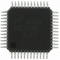
Manufacturer Part Number
MC908AP32CFAE
Description
IC MCU 32K FLASH 8MHZ 48-LQFP
Manufacturer
Freescale Semiconductor
Series
HC08r
Specifications of MC908AP32CFAE
Core Processor
HC08
Core Size
8-Bit
Speed
8MHz
Connectivity
I²C, IRSCI, SCI, SPI
Peripherals
LED, LVD, POR, PWM
Number Of I /o
32
Program Memory Size
32KB (32K x 8)
Program Memory Type
FLASH
Ram Size
2K x 8
Voltage - Supply (vcc/vdd)
2.7 V ~ 5.5 V
Data Converters
A/D 8x10b
Oscillator Type
Internal
Operating Temperature
-40°C ~ 85°C
Package / Case
48-LQFP
Controller Family/series
HC08
No. Of I/o's
32
Ram Memory Size
2KB
Cpu Speed
8MHz
No. Of Timers
2
Embedded Interface Type
I2C, SCI, SPI
Rohs Compliant
Yes
Lead Free Status / RoHS Status
Lead free / RoHS Compliant
Eeprom Size
-
Available stocks
Company
Part Number
Manufacturer
Quantity
Price
Company:

Part Number:
MC908AP32CFAE
Manufacturer:
Freescale Semiconductor
Quantity:
10 000
Company:
Part Number:
MC908AP32CFAER
Manufacturer:
Freescale Semiconductor
Quantity:
10 000


Input/Output (I/O) Ports
SDA and SCL — Multi-Master IIC Data and Clock
TxD and RxD — SCI Transmit and Receive Data
T1CH0 and T1CH1 — Timer 1 Channel I/O
T2CH0 and T2CH1 — Timer 2 Channel I/O
16.3.2 Data Direction Register B (DDRB)
Data direction register B determines whether each port B pin is an input or an output. Writing a logic 1 to
a DDRB bit enables the output buffer for the corresponding port B pin; a logic 0 disables the output buffer.
DDRB[7:0] — Data Direction Register B Bits
Figure 16-8
264
The SDA and SCL pins are multi-master IIC data and clock pins. Setting the MMEN bit in the MMIIC
control register 1 (MMCR1) configures the PTB0/SDA and PTB1/SCL pins for MMIIC function and
overrides any control from the port I/O logic.
The TxD and RxD pins are SCI transmit and receive data pins. Setting the ENSCI bit in the SCI control
register 1 (SCC1) configures the PTB2/TxD and PTB3/RxD pins for SCI function and overrides any
control from the port I/O logic.
The T1CH0 and T1CH1 pins are the TIM1 input capture/output compare pins. The edge/level select
bits, ELSxB:ELSxA, determine whether the PTB4/T1CH0–PTB5/T1CH1 pins are timer channel I/O
pins or general-purpose I/O pins.
The T2CH0 and T2CH1 pins are the TIM2 input capture/output compare pins. The edge/level select
bits, ELSxB:ELSxA, determine whether the PTB6/T2CH0–PTB7/T2CH1 pins are timer channel I/O
pins or general-purpose I/O pins.
These read/write bits control port B data direction. Reset clears DDRB[7:0], configuring all port B pins
as inputs.
1 = Corresponding port B pin configured as output
0 = Corresponding port B pin configured as input
shows the port B I/O logic.
Address:
Avoid glitches on port B pins by writing to the port B data register before
changing data direction register B bits from 0 to 1.
Reset:
Read:
Write:
DDRB7
$0005
Bit 7
0
Figure 16-7. Data Direction Register B (DDRB)
DDRB6
6
0
MC68HC908AP Family Data Sheet, Rev. 4
DDRB5
5
0
NOTE
DDRB4
4
0
DDRB3
3
0
DDRB2
2
0
DDRB1
1
0
Freescale Semiconductor
DDRB0
Bit 0
0
Related parts for MC908AP32CFAE
Image
Part Number
Description
Manufacturer
Datasheet
Request
R

Part Number:
Description:
Manufacturer:
Freescale Semiconductor, Inc
Datasheet:
Part Number:
Description:
Manufacturer:
Freescale Semiconductor, Inc
Datasheet:
Part Number:
Description:
Manufacturer:
Freescale Semiconductor, Inc
Datasheet:
Part Number:
Description:
Manufacturer:
Freescale Semiconductor, Inc
Datasheet:
Part Number:
Description:
Manufacturer:
Freescale Semiconductor, Inc
Datasheet:
Part Number:
Description:
Manufacturer:
Freescale Semiconductor, Inc
Datasheet:
Part Number:
Description:
Manufacturer:
Freescale Semiconductor, Inc
Datasheet:
Part Number:
Description:
Manufacturer:
Freescale Semiconductor, Inc
Datasheet:
Part Number:
Description:
Manufacturer:
Freescale Semiconductor, Inc
Datasheet:
Part Number:
Description:
Manufacturer:
Freescale Semiconductor, Inc
Datasheet:
Part Number:
Description:
Manufacturer:
Freescale Semiconductor, Inc
Datasheet:
Part Number:
Description:
Manufacturer:
Freescale Semiconductor, Inc
Datasheet:
Part Number:
Description:
Manufacturer:
Freescale Semiconductor, Inc
Datasheet:
Part Number:
Description:
Manufacturer:
Freescale Semiconductor, Inc
Datasheet:
Part Number:
Description:
Manufacturer:
Freescale Semiconductor, Inc
Datasheet: