MC908AP32CFAE Freescale Semiconductor, MC908AP32CFAE Datasheet - Page 254
MC908AP32CFAE
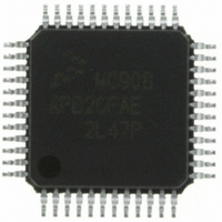
Manufacturer Part Number
MC908AP32CFAE
Description
IC MCU 32K FLASH 8MHZ 48-LQFP
Manufacturer
Freescale Semiconductor
Series
HC08r
Specifications of MC908AP32CFAE
Core Processor
HC08
Core Size
8-Bit
Speed
8MHz
Connectivity
I²C, IRSCI, SCI, SPI
Peripherals
LED, LVD, POR, PWM
Number Of I /o
32
Program Memory Size
32KB (32K x 8)
Program Memory Type
FLASH
Ram Size
2K x 8
Voltage - Supply (vcc/vdd)
2.7 V ~ 5.5 V
Data Converters
A/D 8x10b
Oscillator Type
Internal
Operating Temperature
-40°C ~ 85°C
Package / Case
48-LQFP
Controller Family/series
HC08
No. Of I/o's
32
Ram Memory Size
2KB
Cpu Speed
8MHz
No. Of Timers
2
Embedded Interface Type
I2C, SCI, SPI
Rohs Compliant
Yes
Lead Free Status / RoHS Status
Lead free / RoHS Compliant
Eeprom Size
-
Available stocks
Company
Part Number
Manufacturer
Quantity
Price
Company:

Part Number:
MC908AP32CFAE
Manufacturer:
Freescale Semiconductor
Quantity:
10 000
Company:
Part Number:
MC908AP32CFAER
Manufacturer:
Freescale Semiconductor
Quantity:
10 000


Analog-to-Digital Converter (ADC)
15.5.1 Wait Mode
The ADC continues normal operation in wait mode. Any enabled CPU interrupt request from the ADC can
bring the MCU out of wait mode. If the ADC is not required to bring the MCU out of wait mode, power
down the ADC by setting the ADCH[4:0] bits to logic 1’s before executing the WAIT instruction.
15.5.2 Stop Mode
The ADC module is inactive after the execution of a STOP instruction. Any pending conversion is aborted.
ADC conversions resume when the MCU exits stop mode. Allow one conversion cycle to stabilize the
analog circuitry before attempting a new ADC conversion after exiting stop mode.
15.6 I/O Signals
The ADC module has eight channels shared with port A I/O pins.
15.6.1 ADC Voltage In (V
V
15.6.2 ADC Analog Power Pin (V
The ADC analog portion uses V
as V
15.6.3 ADC Analog Ground Pin (V
The ADC analog portion uses V
as V
15.6.4 ADC Voltage Reference High Pin (V
V
voltage potential as V
Specifications).
15.6.5 ADC Voltage Reference Low Pin (V
V
V
252
ADIN
REFH
REFL
SSA
DD
SS
. There will be a finite current associated with V
is the input voltage signal from one of the eight ADC channels to the ADC module.
is the lower reference supply for the ADC. Connect the V
.
. External filtering may be necessary to ensure clean V
is the power supply for setting the reference voltage V
Route V
capacitors as close as possible to the package.
Route V
capacitors as close as possible to the package.
DDA
DDA
REFH
. There will be a finite current associated with V
carefully for maximum noise immunity and place bypass
carefully for maximum noise immunity and place bypass
ADIN
SSA
DDA
MC68HC908AP Family Data Sheet, Rev. 4
)
as its ground pin. Connect the V
as its power pin. Connect the V
DDA
SSA
)
)
NOTE
NOTE
REFL
REFH
REFL
)
)
(see
REFH
DDA
Chapter 22 Electrical
REFL
. Connect the V
for good results.
DDA
SSA
pin to the same voltage potential as
pin to the same voltage potential
pin to the same voltage potential
REFH
(see
REFH
Chapter 22 Electrical
Freescale Semiconductor
Specifications).
pin to the same
Related parts for MC908AP32CFAE
Image
Part Number
Description
Manufacturer
Datasheet
Request
R

Part Number:
Description:
Manufacturer:
Freescale Semiconductor, Inc
Datasheet:
Part Number:
Description:
Manufacturer:
Freescale Semiconductor, Inc
Datasheet:
Part Number:
Description:
Manufacturer:
Freescale Semiconductor, Inc
Datasheet:
Part Number:
Description:
Manufacturer:
Freescale Semiconductor, Inc
Datasheet:
Part Number:
Description:
Manufacturer:
Freescale Semiconductor, Inc
Datasheet:
Part Number:
Description:
Manufacturer:
Freescale Semiconductor, Inc
Datasheet:
Part Number:
Description:
Manufacturer:
Freescale Semiconductor, Inc
Datasheet:
Part Number:
Description:
Manufacturer:
Freescale Semiconductor, Inc
Datasheet:
Part Number:
Description:
Manufacturer:
Freescale Semiconductor, Inc
Datasheet:
Part Number:
Description:
Manufacturer:
Freescale Semiconductor, Inc
Datasheet:
Part Number:
Description:
Manufacturer:
Freescale Semiconductor, Inc
Datasheet:
Part Number:
Description:
Manufacturer:
Freescale Semiconductor, Inc
Datasheet:
Part Number:
Description:
Manufacturer:
Freescale Semiconductor, Inc
Datasheet:
Part Number:
Description:
Manufacturer:
Freescale Semiconductor, Inc
Datasheet:
Part Number:
Description:
Manufacturer:
Freescale Semiconductor, Inc
Datasheet: