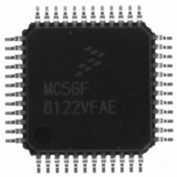
MC56F8122VFAE Freescale Semiconductor, MC56F8122VFAE Datasheet - Page 25

MC56F8122VFAE
Manufacturer Part Number
MC56F8122VFAE
Description
IC DSP 16BIT 40MHZ 48-LQFP
Manufacturer
Freescale Semiconductor
Series
56F8xxxr
Datasheet
1.MC56F8122VFAE.pdf
(136 pages)
Specifications of MC56F8122VFAE
Core Processor
56800
Core Size
16-Bit
Speed
40MHz
Connectivity
SCI, SPI
Peripherals
POR, WDT
Number Of I /o
21
Program Memory Size
32KB (16K x 16)
Program Memory Type
FLASH
Ram Size
4K x 16
Voltage - Supply (vcc/vdd)
2.25 V ~ 3.6 V
Data Converters
A/D 6x12b
Oscillator Type
Internal
Operating Temperature
-40°C ~ 105°C
Package / Case
48-LQFP
Data Bus Width
16 bit
Processor Series
MC56F81xx
Core
56800E
Maximum Clock Frequency
40 MHz
Number Of Programmable I/os
21
Data Ram Size
8 KB
Operating Supply Voltage
- 0.3 V to + 4 V
Maximum Operating Temperature
+ 105 C
Mounting Style
SMD/SMT
Data Rom Size
8 KB
Minimum Operating Temperature
- 40 C
Lead Free Status / RoHS Status
Lead free / RoHS Compliant
Eeprom Size
-
Lead Free Status / Rohs Status
Lead free / RoHS Compliant
Available stocks
Company
Part Number
Manufacturer
Quantity
Price
Company:
Part Number:
MC56F8122VFAE
Manufacturer:
Freescale Semiconductor
Quantity:
10 000
Freescale Semiconductor
Preliminary
Signal Name
FAULTA0
(GPIOA4)
(GPIOA5)
(GPIOA6)
(SCLK1)
PWMA4
(MOSI1)
PWMA5
ANA0
ANA1
ANA2
ANA4
ANA5
ANA6
Table 2-2 Signal and Package Information for the 48-Pin LQFP (Continued)
Pin No.
12
20
21
22
23
24
25
8
9
Schmitt
Schmitt
Schmitt
Schmitt
Schmitt
Schmitt
Output
Output
Output
Output
Output
Output
Output
Input/
Input/
Input/
Input/
Input/
Type
Input
Input
Input
State During
Analog Input ANA0 - 2 — Analog inputs to ADCA, Channel 0
Analog Input ANA4 - 6 — Analog inputs to ADCA, Channel 1
disabled,
pull-up is
disabled,
pull-up is
output is
output is
In reset,
In reset,
enabled
enabled
Reset
56F8322 Technical Data, Rev. 16
Input
PWMA4 — This is one of six PWMA output pins.
SPI 1 Master Out/Slave In — This serial data pin is an output from a
master device and an input to a slave device. The master device
places data on the MOSI line a half-cycle before the clock edge the
slave device uses to latch the data.
Port A GPIO — This GPIO pin can be individually programmed as an
input or output pin.
In the 56F8322, the default state after reset is PWMA4.
In the 56F8122, the default state is not one of the functions offered
and must be reconfigured.
PWMA5 — This is one of six PWMA output pins.
SPI 1 Serial Clock — In the master mode, this pin serves as an
output, clocking slaved listeners. In slave mode, this pin serves as the
data clock input. A Schmitt trigger input is used for noise immunity.
Port A GPIO — This GPIO pin can be individually programmed as an
input or output pin.
In the 56F8322, the default state after reset is PWMA5.
In the 56F8122, the default state is not one of the functions offered
and must be reconfigured.
FAULTA0 — This fault input pin is used for disabling selected PWMA
outputs in cases where fault conditions originate off-chip.
Port A GPIO — This GPIO pin can be individually programmed as an
input or output pin.
In the 56F8322, the default state after reset is FAULTA0.
In the 56F8122, the default state is not one of the functions offered
and must be reconfigured.
Signal Description
Signal Pins
25


