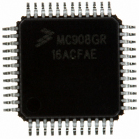
MC908GR16ACFAE Freescale Semiconductor, MC908GR16ACFAE Datasheet - Page 72

MC908GR16ACFAE
Manufacturer Part Number
MC908GR16ACFAE
Description
IC MCU 16K FLASH 8MHZ 48-LQFP
Manufacturer
Freescale Semiconductor
Series
HC08r
Datasheet
1.MC908GR16ACFAE.pdf
(270 pages)
Specifications of MC908GR16ACFAE
Core Processor
HC08
Core Size
8-Bit
Speed
8MHz
Connectivity
LIN, SCI, SPI
Peripherals
LVD, POR, PWM
Number Of I /o
37
Program Memory Size
16KB (16K x 8)
Program Memory Type
FLASH
Ram Size
1K x 8
Voltage - Supply (vcc/vdd)
3 V ~ 5.5 V
Data Converters
A/D 8x10b
Oscillator Type
Internal
Operating Temperature
-40°C ~ 85°C
Package / Case
48-LQFP
Controller Family/series
HC08
No. Of I/o's
37
Ram Memory Size
1KB
Cpu Speed
8MHz
No. Of Timers
2
Embedded Interface Type
SCI, SPI
Rohs Compliant
Yes
Processor Series
HC08GR
Core
HC08
Data Bus Width
8 bit
Data Ram Size
1 KB
Interface Type
ESCI, SPI
Maximum Clock Frequency
8 MHz
Number Of Programmable I/os
37
Number Of Timers
4
Maximum Operating Temperature
+ 85 C
Mounting Style
SMD/SMT
Development Tools By Supplier
FSICEBASE, DEMO908GZ60E, M68CBL05CE, M68EML08GPGTE
Minimum Operating Temperature
- 40 C
On-chip Adc
10 bit, 8 Channel
Lead Free Status / RoHS Status
Lead free / RoHS Compliant
Eeprom Size
-
Lead Free Status / Rohs Status
Details
Available stocks
Company
Part Number
Manufacturer
Quantity
Price
Company:
Part Number:
MC908GR16ACFAE
Manufacturer:
Freescale Semiconductor
Quantity:
10 000
Part Number:
MC908GR16ACFAE
Manufacturer:
FREESCALE
Quantity:
20 000
Company:
Part Number:
MC908GR16ACFAER
Manufacturer:
Freescale Semiconductor
Quantity:
10 000
Clock Generator Module (CGM)
4.7.2 Stop Mode
If the OSCENINSTOP bit in the CONFIG2 register is cleared (default), then the STOP instruction disables
the CGM (oscillator and phase locked loop) and holds low all CGM outputs (CGMXCLK, CGMOUT, and
CGMINT).
If the OSCENINSTOP bit in the CONFIG2 register is set, then the phase locked loop is shut off but the
oscillator will continue to operate in stop mode.
4.7.3 CGM During Break Interrupts
The system integration module (SIM) controls whether status bits in other modules can be cleared during
the break state. The BCFE bit in the SIM break flag control register (SBFCR) enables software to clear
status bits during the break state. See
19.2.2.4 SIM Break Flag Control
Register.
To allow software to clear status bits during a break interrupt, write a 1 to the BCFE bit. If a status bit is
cleared during the break state, it remains cleared when the MCU exits the break state.
To protect the PLLF bit during the break state, write a 0 to the BCFE bit. With BCFE at 0 (its default state),
software can read and write the PLL control register during the break state without affecting the PLLF bit.
4.8 Acquisition/Lock Time Specifications
The acquisition and lock times of the PLL are, in many applications, the most critical PLL design
parameters. Proper design and use of the PLL ensures the highest stability and lowest acquisition/lock
times.
4.8.1 Acquisition/Lock Time Definitions
Typical control systems refer to the acquisition time or lock time as the reaction time, within specified
tolerances, of the system to a step input. In a PLL, the step input occurs when the PLL is turned on or
when it suffers a noise hit. The tolerance is usually specified as a percent of the step input or when the
output settles to the desired value plus or minus a percent of the frequency change. Therefore, the
reaction time is constant in this definition, regardless of the size of the step input. For example, consider
a system with a 5 percent acquisition time tolerance. If a command instructs the system to change from
0 Hz to 1 MHz, the acquisition time is the time taken for the frequency to reach 1 MHz ±50 kHz.
Fifty kHz = 5% of the 1-MHz step input. If the system is operating at 1 MHz and suffers a –100-kHz noise
hit, the acquisition time is the time taken to return from 900 kHz to 1 MHz ±5 kHz. Five kHz = 5% of the
100-kHz step input.
Other systems refer to acquisition and lock times as the time the system takes to reduce the error between
the actual output and the desired output to within specified tolerances. Therefore, the acquisition or lock
time varies according to the original error in the output. Minor errors may not even be registered. Typical
PLL applications prefer to use this definition because the system requires the output frequency to be
within a certain tolerance of the desired frequency regardless of the size of the initial error.
4.8.2 Parametric Influences on Reaction Time
Acquisition and lock times are designed to be as short as possible while still providing the highest possible
stability. These reaction times are not constant, however. Many factors directly and indirectly affect the
acquisition time.
MC68HC908GR16A Data Sheet, Rev. 1.0
72
Freescale Semiconductor


