C8051F34B-GQ Silicon Laboratories Inc, C8051F34B-GQ Datasheet - Page 10
C8051F34B-GQ
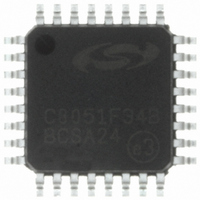
Manufacturer Part Number
C8051F34B-GQ
Description
IC 8051 MCU 32K FLASH 32LQFP
Manufacturer
Silicon Laboratories Inc
Series
C8051F34xr
Datasheet
1.C8051F349-GQ.pdf
(276 pages)
Specifications of C8051F34B-GQ
Program Memory Type
FLASH
Program Memory Size
32KB (32K x 8)
Package / Case
32-LQFP
Core Processor
8051
Core Size
8-Bit
Speed
48MHz
Connectivity
SMBus (2-Wire/I²C), SPI, UART/USART, USB
Peripherals
Brown-out Detect/Reset, POR, PWM, Temp Sensor, WDT
Number Of I /o
25
Ram Size
2.25K x 8
Voltage - Supply (vcc/vdd)
2.7 V ~ 3.6 V
Data Converters
A/D 17x10b
Oscillator Type
Internal
Operating Temperature
-40°C ~ 85°C
Processor Series
C8051F3x
Core
8051
Data Bus Width
8 bit
Data Ram Size
2.25 KB
Interface Type
I2C/SMBus/SPI/UART/USB
Maximum Clock Frequency
48 MHz
Number Of Programmable I/os
25
Number Of Timers
4
Maximum Operating Temperature
+ 85 C
Mounting Style
SMD/SMT
3rd Party Development Tools
KSK-SL-F34X, KSK-SL-TOOLSTICK, PK51, CA51, A51, ULINK2
Development Tools By Supplier
C8051F340DK
Minimum Operating Temperature
- 40 C
Package
32LQFP
Device Core
8051
Family Name
C8051F34x
Maximum Speed
48 MHz
Operating Supply Voltage
3.3|5 V
On-chip Adc
17-chx10-bit
Lead Free Status / RoHS Status
Lead free / RoHS Compliant
For Use With
336-1748 - ADAPTER TOOLSTICK FOR C8051F34X
Eeprom Size
-
Lead Free Status / Rohs Status
Lead free / RoHS Compliant
Other names
336-1534
Available stocks
Company
Part Number
Manufacturer
Quantity
Price
Company:

Part Number:
C8051F34B-GQ
Manufacturer:
Silicon Laboratories Inc
Quantity:
10 000
Company:
Part Number:
C8051F34B-GQR
Manufacturer:
Silicon Laboratories Inc
Quantity:
10 000


C8051F340/1/2/3/4/5/6/7/8/9/A/B/C/D
20. Enhanced Serial Peripheral Interface (SPI0)
21. Timers
22. Programmable Counter Array (PCA0)
23. C2 Interface
10
Figure 19.1. UART1 Block Diagram ....................................................................... 213
Figure 19.2. UART1 Timing Without Parity or Extra Bit.......................................... 215
Figure 19.3. UART1 Timing With Parity ................................................................. 215
Figure 19.4. UART1 Timing With Extra Bit ............................................................. 215
Figure 19.5. Typical UART Interconnect Diagram.................................................. 216
Figure 19.6. UART Multi-Processor Mode Interconnect Diagram .......................... 218
Figure 20.1. SPI Block Diagram ............................................................................. 222
Figure 20.2. Multiple-Master Mode Connection Diagram ....................................... 225
Figure 20.3. 3-Wire Single Master and Slave Mode Connection Diagram ............. 225
Figure 20.4. 4-Wire Single Master Mode and Slave Mode Connection Diagram ... 225
Figure 20.5. Master Mode Data/Clock Timing ........................................................ 227
Figure 20.6. Slave Mode Data/Clock Timing (CKPHA = 0) .................................... 228
Figure 20.7. Slave Mode Data/Clock Timing (CKPHA = 1) .................................... 228
Figure 20.8. SPI Master Timing (CKPHA = 0)........................................................ 232
Figure 20.9. SPI Master Timing (CKPHA = 1)........................................................ 232
Figure 20.10. SPI Slave Timing (CKPHA = 0)........................................................ 233
Figure 20.11. SPI Slave Timing (CKPHA = 1)........................................................ 233
Figure 21.1. T0 Mode 0 Block Diagram.................................................................. 236
Figure 21.2. T0 Mode 2 Block Diagram.................................................................. 237
Figure 21.3. T0 Mode 3 Block Diagram.................................................................. 238
Figure 21.4. Timer 2 16-Bit Mode Block Diagram .................................................. 243
Figure 21.5. Timer 2 8-Bit Mode Block Diagram .................................................... 244
Figure 21.6. Timer 2 Capture Mode (T2SPLIT = ‘0’) .............................................. 245
Figure 21.7. Timer 2 Capture Mode (T2SPLIT = ‘1’) .............................................. 246
Figure 21.8. Timer 3 16-Bit Mode Block Diagram .................................................. 249
Figure 21.9. Timer 3 8-Bit Mode Block Diagram .................................................... 250
Figure 21.10. Timer 3 Capture Mode (T3SPLIT = ‘0’) ............................................ 251
Figure 21.11. Timer 3 Capture Mode (T3SPLIT = ‘1’) ............................................ 252
Figure 22.1. PCA Block Diagram............................................................................ 255
Figure 22.2. PCA Counter/Timer Block Diagram.................................................... 256
Figure 22.3. PCA Interrupt Block Diagram ............................................................. 257
Figure 22.4. PCA Capture Mode Diagram.............................................................. 258
Figure 22.5. PCA Software Timer Mode Diagram .................................................. 259
Figure 22.6. PCA High Speed Output Mode Diagram............................................ 260
Figure 22.7. PCA Frequency Output Mode ............................................................ 261
Figure 22.8. PCA 8-Bit PWM Mode Diagram ......................................................... 262
Figure 22.9. PCA 16-Bit PWM Mode...................................................................... 263
Figure 22.10. PCA Module 4 with Watchdog Timer Enabled ................................. 264
Figure 23.1. Typical C2 Pin Sharing....................................................................... 273
Rev. 1.3
Related parts for C8051F34B-GQ
Image
Part Number
Description
Manufacturer
Datasheet
Request
R

Part Number:
Description:
SMD/C°/SINGLE-ENDED OUTPUT SILICON OSCILLATOR
Manufacturer:
Silicon Laboratories Inc
Part Number:
Description:
Manufacturer:
Silicon Laboratories Inc
Datasheet:
Part Number:
Description:
N/A N/A/SI4010 AES KEYFOB DEMO WITH LCD RX
Manufacturer:
Silicon Laboratories Inc
Datasheet:
Part Number:
Description:
N/A N/A/SI4010 SIMPLIFIED KEY FOB DEMO WITH LED RX
Manufacturer:
Silicon Laboratories Inc
Datasheet:
Part Number:
Description:
N/A/-40 TO 85 OC/EZLINK MODULE; F930/4432 HIGH BAND (REV E/B1)
Manufacturer:
Silicon Laboratories Inc
Part Number:
Description:
EZLink Module; F930/4432 Low Band (rev e/B1)
Manufacturer:
Silicon Laboratories Inc
Part Number:
Description:
I°/4460 10 DBM RADIO TEST CARD 434 MHZ
Manufacturer:
Silicon Laboratories Inc
Part Number:
Description:
I°/4461 14 DBM RADIO TEST CARD 868 MHZ
Manufacturer:
Silicon Laboratories Inc
Part Number:
Description:
I°/4463 20 DBM RFSWITCH RADIO TEST CARD 460 MHZ
Manufacturer:
Silicon Laboratories Inc
Part Number:
Description:
I°/4463 20 DBM RADIO TEST CARD 868 MHZ
Manufacturer:
Silicon Laboratories Inc
Part Number:
Description:
I°/4463 27 DBM RADIO TEST CARD 868 MHZ
Manufacturer:
Silicon Laboratories Inc
Part Number:
Description:
I°/4463 SKYWORKS 30 DBM RADIO TEST CARD 915 MHZ
Manufacturer:
Silicon Laboratories Inc
Part Number:
Description:
N/A N/A/-40 TO 85 OC/4463 RFMD 30 DBM RADIO TEST CARD 915 MHZ
Manufacturer:
Silicon Laboratories Inc
Part Number:
Description:
I°/4463 20 DBM RADIO TEST CARD 169 MHZ
Manufacturer:
Silicon Laboratories Inc