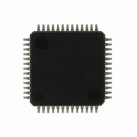
R5F21256SNFP#U0 Renesas Electronics America, R5F21256SNFP#U0 Datasheet - Page 372

R5F21256SNFP#U0
Manufacturer Part Number
R5F21256SNFP#U0
Description
IC R8C MCU FLASH 32K 52LQFP
Manufacturer
Renesas Electronics America
Series
R8C/2x/25r
Datasheets
1.R5F211A2SPU0.pdf
(300 pages)
2.R5F21246SDFPU0.pdf
(61 pages)
3.R5F21246SDFPU0.pdf
(527 pages)
Specifications of R5F21256SNFP#U0
Core Processor
R8C
Core Size
16/32-Bit
Speed
20MHz
Connectivity
I²C, LIN, SIO, SSU, UART/USART
Peripherals
POR, Voltage Detect, WDT
Number Of I /o
41
Program Memory Size
32KB (32K x 8)
Program Memory Type
FLASH
Ram Size
2K x 8
Voltage - Supply (vcc/vdd)
2.2 V ~ 5.5 V
Data Converters
A/D 12x10b
Oscillator Type
Internal
Operating Temperature
-20°C ~ 85°C
Package / Case
52-LQFP
For Use With
R0K521256S000BE - KIT EVAL STARTER FOR R8C/25
Lead Free Status / RoHS Status
Lead free / RoHS Compliant
Eeprom Size
-
Available stocks
Company
Part Number
Manufacturer
Quantity
Price
Part Number:
R5F21256SNFP#U0R5F21256SNFP#ES
Manufacturer:
Renesas Electronics America
Quantity:
10 000
- Current page: 372 of 527
- Download datasheet (6Mb)
R8C/24 Group, R8C/25 Group
Rev.3.00
REJ09B0244-0300
16.3.3.4
In slave transmit mode, the slave device outputs the transmit data while the master device outputs the receive
clock and returns an acknowledge signal.
Figures 16.37 and 16.38 show the Operating Timing in Slave Transmit Mode (I
The transmit procedure and operation in slave transmit mode are as follows.
(1) Set the ICE bit in the ICCR1 register to 1 (transfer operation enabled). Set bits WAIT and MLS in the
(2) When the slave address matches at the 1st frame after detecting the start condition, the slave device
(3) When the TDRE bit in the ICDRT register is set to 1 after writing the last transmit data to the ICDRT
(4) The SCL signal is released by setting the TRS bit to 0 and performing a dummy read of the ICDRR
(5) Set the TDRE bit to 0.
Feb 29, 2008
ICMR register and bits CKS0 to CKS3 in the ICCR1 register (initial setting). Set bits TRS and MST in
the ICCR1 register to 0 and wait until the slave address matches in slave receive mode.
outputs the level set by the ACKBT bit in the ICIER register to the SDA pin at the rise of the 9th clock
cycle. At this time, if the 8th bit of data (R/W) is 1, bits TRS and TDRE in the ICSR register are set to 1,
and the mode is switched to slave transmit mode automatically. Continuous transmission is enabled by
writing transmit data to the ICDRT register every time the TDRE bit is set to 1.
register, wait until the TEND bit in the ICSR register is set to 1 while the TDRE bit is set to 1. When the
TEND bit is set to 1, set the TEND bit to 0.
register to end the process.
Slave Transmit Operation
Page 353 of 485
16. Clock Synchronous Serial Interface
2
C bus Interface Mode).
Related parts for R5F21256SNFP#U0
Image
Part Number
Description
Manufacturer
Datasheet
Request
R

Part Number:
Description:
KIT STARTER FOR M16C/29
Manufacturer:
Renesas Electronics America
Datasheet:

Part Number:
Description:
KIT STARTER FOR R8C/2D
Manufacturer:
Renesas Electronics America
Datasheet:

Part Number:
Description:
R0K33062P STARTER KIT
Manufacturer:
Renesas Electronics America
Datasheet:

Part Number:
Description:
KIT STARTER FOR R8C/23 E8A
Manufacturer:
Renesas Electronics America
Datasheet:

Part Number:
Description:
KIT STARTER FOR R8C/25
Manufacturer:
Renesas Electronics America
Datasheet:

Part Number:
Description:
KIT STARTER H8S2456 SHARPE DSPLY
Manufacturer:
Renesas Electronics America
Datasheet:

Part Number:
Description:
KIT STARTER FOR R8C38C
Manufacturer:
Renesas Electronics America
Datasheet:

Part Number:
Description:
KIT STARTER FOR R8C35C
Manufacturer:
Renesas Electronics America
Datasheet:

Part Number:
Description:
KIT STARTER FOR R8CL3AC+LCD APPS
Manufacturer:
Renesas Electronics America
Datasheet:

Part Number:
Description:
KIT STARTER FOR RX610
Manufacturer:
Renesas Electronics America
Datasheet:

Part Number:
Description:
KIT STARTER FOR R32C/118
Manufacturer:
Renesas Electronics America
Datasheet:

Part Number:
Description:
KIT DEV RSK-R8C/26-29
Manufacturer:
Renesas Electronics America
Datasheet:

Part Number:
Description:
KIT STARTER FOR SH7124
Manufacturer:
Renesas Electronics America
Datasheet:

Part Number:
Description:
KIT STARTER FOR H8SX/1622
Manufacturer:
Renesas Electronics America
Datasheet:

Part Number:
Description:
KIT DEV FOR SH7203
Manufacturer:
Renesas Electronics America
Datasheet:


