R5F21184SP#U0 Renesas Electronics America, R5F21184SP#U0 Datasheet - Page 49
R5F21184SP#U0
Manufacturer Part Number
R5F21184SP#U0
Description
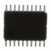
IC R8C MCU FLASH 16K 20SSOP
Manufacturer
Renesas Electronics America
Series
M16C™ M16C/R8C/Tiny/18r
Datasheets
1.R5F211A2SPU0.pdf
(300 pages)
2.R5F21181DSPU0.pdf
(43 pages)
3.R5F21181DSPU0.pdf
(259 pages)
Specifications of R5F21184SP#U0
Core Size
16-Bit
Program Memory Size
16KB (16K x 8)
Core Processor
R8C
Speed
20MHz
Connectivity
SIO, UART/USART
Peripherals
LED, POR, Voltage Detect, WDT
Number Of I /o
13
Program Memory Type
FLASH
Ram Size
1K x 8
Voltage - Supply (vcc/vdd)
2.7 V ~ 5.5 V
Data Converters
A/D 4x1b
Oscillator Type
Internal
Operating Temperature
-20°C ~ 85°C
Package / Case
20-SSOP
No. Of I/o's
13
Ram Memory Size
1KB
Cpu Speed
20MHz
No. Of Timers
3
Digital Ic Case Style
SSOP
Supply Voltage Range
2.7V To 5.5V
Embedded Interface Type
UART
Rohs Compliant
Yes
Lead Free Status / RoHS Status
Lead free / RoHS Compliant
For Use With
R0K521134S000BE - KIT EVAL STARTER FOR R8C/13R0E521174CPE10 - EMULATOR COMPACT R8C/18/19/1
Eeprom Size
-
Lead Free Status / RoHS Status
Lead free / RoHS Compliant, Lead free / RoHS Compliant


Rev.2.00 Oct 17, 2005
REJ09B0001-0200
Chapter 2 Addressing Modes
label
Program counter relative
• If the jump length specifier (.length)
is (.S), the base address plus the
value indicated by the displacement
(dsp)—added without the sign bits—is
the effective address.
This addressing mode can be used
with the JMP instruction.
• If the jump length specifier (.length) is
(.B) or (.W), the base address plus the
value indicated by the displacement
(dsp)—added including the sign bits—is
the effective address.
However, if the addition results in a value
outside the range 00000
bits 21 and above are ignored, and the
address returns to 00000
This addressing mode can be used with
the JMP and JSR instructions.
page 29 of 263
16
16
to FFFFF
or FFFFF
16
16
,
.
*1 The base address is (start address of instruction + 2).
If the dsp value is positive
If the specifier is (.B), -128 dsp +127
If the specifier is (.W), -32768 dsp +32767
*2 The base address varies depending on the instruction.
If the dsp value is negative
dsp
dsp
dsp
Base address
Base address
2.4 Special Instruction Addressing
+0
dsp +7
label
label
label
Memory
Memory
Related parts for R5F21184SP#U0
Image
Part Number
Description
Manufacturer
Datasheet
Request
R

Part Number:
Description:
KIT STARTER FOR M16C/29
Manufacturer:
Renesas Electronics America
Datasheet:

Part Number:
Description:
KIT STARTER FOR R8C/2D
Manufacturer:
Renesas Electronics America
Datasheet:

Part Number:
Description:
R0K33062P STARTER KIT
Manufacturer:
Renesas Electronics America
Datasheet:

Part Number:
Description:
KIT STARTER FOR R8C/23 E8A
Manufacturer:
Renesas Electronics America
Datasheet:

Part Number:
Description:
KIT STARTER FOR R8C/25
Manufacturer:
Renesas Electronics America
Datasheet:

Part Number:
Description:
KIT STARTER H8S2456 SHARPE DSPLY
Manufacturer:
Renesas Electronics America
Datasheet:

Part Number:
Description:
KIT STARTER FOR R8C38C
Manufacturer:
Renesas Electronics America
Datasheet:

Part Number:
Description:
KIT STARTER FOR R8C35C
Manufacturer:
Renesas Electronics America
Datasheet:

Part Number:
Description:
KIT STARTER FOR R8CL3AC+LCD APPS
Manufacturer:
Renesas Electronics America
Datasheet:
Part Number:
Description:
KIT STARTER FOR RX610
Manufacturer:
Renesas Electronics America
Datasheet:

Part Number:
Description:
KIT STARTER FOR R32C/118
Manufacturer:
Renesas Electronics America
Datasheet:

Part Number:
Description:
KIT DEV RSK-R8C/26-29
Manufacturer:
Renesas Electronics America
Datasheet:

Part Number:
Description:
KIT STARTER FOR SH7124
Manufacturer:
Renesas Electronics America
Datasheet:

Part Number:
Description:
KIT STARTER FOR H8SX/1622
Manufacturer:
Renesas Electronics America
Datasheet:

Part Number:
Description:
KIT DEV FOR SH7203
Manufacturer:
Renesas Electronics America
Datasheet: