C8051F819-GM Silicon Laboratories Inc, C8051F819-GM Datasheet - Page 8
C8051F819-GM
Manufacturer Part Number
C8051F819-GM
Description
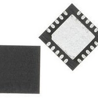
IC MCU 8BIT 8KB FLASH 20QFN
Manufacturer
Silicon Laboratories Inc
Series
C8051F81xr
Datasheet
1.C8051F800DK.pdf
(250 pages)
Specifications of C8051F819-GM
Core Processor
8051
Core Size
8-Bit
Speed
25MHz
Connectivity
SMBus (2-Wire/I²C), SPI, UART/USART
Peripherals
Cap Sense, POR, PWM, WDT
Number Of I /o
17
Program Memory Size
8KB (8K x 8)
Program Memory Type
FLASH
Ram Size
512 x 8
Voltage - Supply (vcc/vdd)
1.8 V ~ 3.6 V
Oscillator Type
Internal
Operating Temperature
-40°C ~ 85°C
Package / Case
20-QFN
Processor Series
C8051F8x
Core
8051
Data Bus Width
16 bit
Data Ram Size
512 B
Interface Type
I2C, SPI, UART
Maximum Clock Frequency
25 MHz
Number Of Programmable I/os
17
Number Of Timers
3
Operating Supply Voltage
1.8 V to 3.6 V
Maximum Operating Temperature
+ 125 C
Mounting Style
SMD/SMT
3rd Party Development Tools
PK51, CA51, A51, ULINK2
Development Tools By Supplier
C8051F800DK
Minimum Operating Temperature
- 55 C
Package
20QFN EP
Device Core
8051
Family Name
C8051F8xx
Maximum Speed
25 MHz
Lead Free Status / RoHS Status
Lead free / RoHS Compliant
Eeprom Size
-
Data Converters
-
Lead Free Status / Rohs Status
Details
Other names
336-1799-5


C8051F80x-83x
19. Flash Memory
20. Power Management Modes
21. Reset Sources
22. Oscillators and Clock Selection
23. Port Input/Output
24. Cyclic Redundancy Check Unit (CRC0)
25. Enhanced Serial Peripheral Interface (SPI0)
26. SMBus
27. UART0
28. Timers
29. Programmable Counter Array
30. C2 Interface
8
Table 18.1. Interrupt Summary .............................................................................. 104
Table 19.1. Flash Security Summary .................................................................... 115
Table 23.1. Port I/O Assignment for Analog Functions ......................................... 141
Table 23.2. Port I/O Assignment for Digital Functions ........................................... 142
Table 23.3. Port I/O Assignment for External Digital Event Capture Functions .... 142
Table 24.1. Example 16-bit CRC Outputs ............................................................. 160
Table 24.2. Example 32-bit CRC Outputs ............................................................. 161
Table 25.1. SPI Slave Timing Parameters ............................................................ 179
Table 26.1. SMBus Clock Source Selection .......................................................... 184
Table 26.2. Minimum SDA Setup and Hold Times ................................................ 185
Table 26.3. Sources for Hardware Changes to SMB0CN ..................................... 189
Table 26.4. Hardware Address Recognition Examples (EHACK = 1) ................... 190
Table 26.5. SMBus Status Decoding With Hardware ACK Generation Disabled
Table 26.6. SMBus Status Decoding With Hardware ACK Generation Enabled
Table 27.1. Timer Settings for Standard Baud Rates
Table 27.2. Timer Settings for Standard Baud Rates
Table 29.1. PCA Timebase Input Options ............................................................. 226
Table 29.2. PCA0CPM and PCA0PWM Bit Settings for PCA Capture/Compare
Table 29.3. Watchdog Timer Timeout Intervals1 ................................................... 237
(EHACK = 0) ....................................................................................... 197
(EHACK = 1) ....................................................................................... 199
Using The Internal 24.5 MHz Oscillator .............................................. 208
Using an External 22.1184 MHz Oscillator ......................................... 208
Modules
1,2,3,4,5,6
................................................................................. 228
Rev. 1.0
Related parts for C8051F819-GM
Image
Part Number
Description
Manufacturer
Datasheet
Request
R

Part Number:
Description:
SMD/C°/SINGLE-ENDED OUTPUT SILICON OSCILLATOR
Manufacturer:
Silicon Laboratories Inc
Part Number:
Description:
Manufacturer:
Silicon Laboratories Inc
Datasheet:
Part Number:
Description:
N/A N/A/SI4010 AES KEYFOB DEMO WITH LCD RX
Manufacturer:
Silicon Laboratories Inc
Datasheet:
Part Number:
Description:
N/A N/A/SI4010 SIMPLIFIED KEY FOB DEMO WITH LED RX
Manufacturer:
Silicon Laboratories Inc
Datasheet:
Part Number:
Description:
N/A/-40 TO 85 OC/EZLINK MODULE; F930/4432 HIGH BAND (REV E/B1)
Manufacturer:
Silicon Laboratories Inc
Part Number:
Description:
EZLink Module; F930/4432 Low Band (rev e/B1)
Manufacturer:
Silicon Laboratories Inc
Part Number:
Description:
I°/4460 10 DBM RADIO TEST CARD 434 MHZ
Manufacturer:
Silicon Laboratories Inc
Part Number:
Description:
I°/4461 14 DBM RADIO TEST CARD 868 MHZ
Manufacturer:
Silicon Laboratories Inc
Part Number:
Description:
I°/4463 20 DBM RFSWITCH RADIO TEST CARD 460 MHZ
Manufacturer:
Silicon Laboratories Inc
Part Number:
Description:
I°/4463 20 DBM RADIO TEST CARD 868 MHZ
Manufacturer:
Silicon Laboratories Inc
Part Number:
Description:
I°/4463 27 DBM RADIO TEST CARD 868 MHZ
Manufacturer:
Silicon Laboratories Inc
Part Number:
Description:
I°/4463 SKYWORKS 30 DBM RADIO TEST CARD 915 MHZ
Manufacturer:
Silicon Laboratories Inc
Part Number:
Description:
N/A N/A/-40 TO 85 OC/4463 RFMD 30 DBM RADIO TEST CARD 915 MHZ
Manufacturer:
Silicon Laboratories Inc
Part Number:
Description:
I°/4463 20 DBM RADIO TEST CARD 169 MHZ
Manufacturer:
Silicon Laboratories Inc