C8051F819-GM Silicon Laboratories Inc, C8051F819-GM Datasheet - Page 152
C8051F819-GM
Manufacturer Part Number
C8051F819-GM
Description
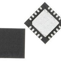
IC MCU 8BIT 8KB FLASH 20QFN
Manufacturer
Silicon Laboratories Inc
Series
C8051F81xr
Datasheet
1.C8051F800DK.pdf
(250 pages)
Specifications of C8051F819-GM
Core Processor
8051
Core Size
8-Bit
Speed
25MHz
Connectivity
SMBus (2-Wire/I²C), SPI, UART/USART
Peripherals
Cap Sense, POR, PWM, WDT
Number Of I /o
17
Program Memory Size
8KB (8K x 8)
Program Memory Type
FLASH
Ram Size
512 x 8
Voltage - Supply (vcc/vdd)
1.8 V ~ 3.6 V
Oscillator Type
Internal
Operating Temperature
-40°C ~ 85°C
Package / Case
20-QFN
Processor Series
C8051F8x
Core
8051
Data Bus Width
16 bit
Data Ram Size
512 B
Interface Type
I2C, SPI, UART
Maximum Clock Frequency
25 MHz
Number Of Programmable I/os
17
Number Of Timers
3
Operating Supply Voltage
1.8 V to 3.6 V
Maximum Operating Temperature
+ 125 C
Mounting Style
SMD/SMT
3rd Party Development Tools
PK51, CA51, A51, ULINK2
Development Tools By Supplier
C8051F800DK
Minimum Operating Temperature
- 55 C
Package
20QFN EP
Device Core
8051
Family Name
C8051F8xx
Maximum Speed
25 MHz
Lead Free Status / RoHS Status
Lead free / RoHS Compliant
Eeprom Size
-
Data Converters
-
Lead Free Status / Rohs Status
Details
Other names
336-1799-5


C8051F80x-83x
SFR Definition 23.5. P1MASK: Port 1 Mask Register
SFR Address = 0xEE
SFR Definition 23.6. P1MAT: Port 1 Match Register
SFR Address = 0xED
23.6. Special Function Registers for Accessing and Configuring Port I/O
All Port I/O are accessed through corresponding special function registers (SFRs) that are both byte
addressable and bit addressable. When writing to a Port, the value written to the SFR is latched to main-
tain the output data value at each pin. When reading, the logic levels of the Port's input pins are returned
regardless of the XBRn settings (i.e., even when the pin is assigned to another signal by the Crossbar, the
Port register can always read its corresponding Port I/O pin). The exception to this is the execution of the
read-modify-write instructions that target a Port Latch register as the destination. The read-modify-write
instructions when operating on a Port SFR are the following: ANL, ORL, XRL, JBC, CPL, INC, DEC, DJNZ
and MOV, CLR or SETB, when the destination is an individual bit in a Port SFR. For these instructions, the
value of the latch register (not the pin) is read, modified, and written back to the SFR.
152
Name
Reset
Name
Reset
7:0
7:0
Bit
Bit
Type
Type
Bit
Bit
P1MASK[7:0]
P1MAT[7:0]
Name
Name
7
0
7
1
Port 1 Mask Value.
Selects P1 pins to be compared to the corresponding bits in P1MAT.
0: P1.n pin logic value is ignored and cannot cause a Port Mismatch event.
1: P1.n pin logic value is compared to P1MAT.n.
Note: P1.4–P1.7 are not available on 16-pin packages.
Port 1 Match Value.
Match comparison value used on Port 1 for bits in P1MASK which are set to 1.
0: P1.n pin logic value is compared with logic LOW.
1: P1.n pin logic value is compared with logic HIGH.
Note: P1.4–P1.7 are not available on 16-pin packages.
6
0
6
1
5
0
5
1
Rev. 1.0
4
P1MASK[7:0]
0
4
1
P1MAT[7:0]
R/W
R/W
Function
Function
3
0
3
1
2
0
2
1
1
0
1
1
0
0
0
1
Related parts for C8051F819-GM
Image
Part Number
Description
Manufacturer
Datasheet
Request
R

Part Number:
Description:
SMD/C°/SINGLE-ENDED OUTPUT SILICON OSCILLATOR
Manufacturer:
Silicon Laboratories Inc
Part Number:
Description:
Manufacturer:
Silicon Laboratories Inc
Datasheet:
Part Number:
Description:
N/A N/A/SI4010 AES KEYFOB DEMO WITH LCD RX
Manufacturer:
Silicon Laboratories Inc
Datasheet:
Part Number:
Description:
N/A N/A/SI4010 SIMPLIFIED KEY FOB DEMO WITH LED RX
Manufacturer:
Silicon Laboratories Inc
Datasheet:
Part Number:
Description:
N/A/-40 TO 85 OC/EZLINK MODULE; F930/4432 HIGH BAND (REV E/B1)
Manufacturer:
Silicon Laboratories Inc
Part Number:
Description:
EZLink Module; F930/4432 Low Band (rev e/B1)
Manufacturer:
Silicon Laboratories Inc
Part Number:
Description:
I°/4460 10 DBM RADIO TEST CARD 434 MHZ
Manufacturer:
Silicon Laboratories Inc
Part Number:
Description:
I°/4461 14 DBM RADIO TEST CARD 868 MHZ
Manufacturer:
Silicon Laboratories Inc
Part Number:
Description:
I°/4463 20 DBM RFSWITCH RADIO TEST CARD 460 MHZ
Manufacturer:
Silicon Laboratories Inc
Part Number:
Description:
I°/4463 20 DBM RADIO TEST CARD 868 MHZ
Manufacturer:
Silicon Laboratories Inc
Part Number:
Description:
I°/4463 27 DBM RADIO TEST CARD 868 MHZ
Manufacturer:
Silicon Laboratories Inc
Part Number:
Description:
I°/4463 SKYWORKS 30 DBM RADIO TEST CARD 915 MHZ
Manufacturer:
Silicon Laboratories Inc
Part Number:
Description:
N/A N/A/-40 TO 85 OC/4463 RFMD 30 DBM RADIO TEST CARD 915 MHZ
Manufacturer:
Silicon Laboratories Inc
Part Number:
Description:
I°/4463 20 DBM RADIO TEST CARD 169 MHZ
Manufacturer:
Silicon Laboratories Inc