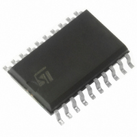
ST7FLIT19BF1M6 STMicroelectronics, ST7FLIT19BF1M6 Datasheet - Page 84

ST7FLIT19BF1M6
Manufacturer Part Number
ST7FLIT19BF1M6
Description
IC MCU 8BIT 4K FLASH 20SOIC
Manufacturer
STMicroelectronics
Series
ST7r
Datasheet
1.ST7FLIT15BY1M6.pdf
(159 pages)
Specifications of ST7FLIT19BF1M6
Core Processor
ST7
Core Size
8-Bit
Speed
8MHz
Connectivity
SPI
Peripherals
LVD, POR, PWM, WDT
Number Of I /o
17
Program Memory Size
4KB (4K x 8)
Program Memory Type
FLASH
Eeprom Size
128 x 8
Ram Size
256 x 8
Voltage - Supply (vcc/vdd)
2.7 V ~ 5.5 V
Data Converters
A/D 7x10b
Oscillator Type
Internal
Operating Temperature
-40°C ~ 85°C
Package / Case
20-SOIC (7.5mm Width)
Processor Series
ST7FLIT1x
Core
ST7
Data Bus Width
8 bit
Data Ram Size
256 B
Interface Type
SPI
Maximum Clock Frequency
8 MHz
Number Of Programmable I/os
17
Number Of Timers
4
Operating Supply Voltage
2.7 V to 5.5 V
Maximum Operating Temperature
+ 85 C
Mounting Style
SMD/SMT
Development Tools By Supplier
ST7FLITE-SK/RAIS, ST7FLIT1B-D/RAIS, ST7MDT10-DVP3, ST7MDT10-EMU3, STX-RLINK
Minimum Operating Temperature
- 40 C
On-chip Adc
10 bit, 7 Channel
For Use With
497-6232 - BOARD EVAL ST7LITE1B,STP5NK60Z497-5049 - KIT STARTER RAISONANCE ST7FLITE497-5046 - KIT TOOL FOR ST7/UPSD/STR7 MCU
Lead Free Status / RoHS Status
Lead free / RoHS Compliant
Other names
497-5627-5
- Current page: 84 of 159
- Download datasheet (3Mb)
ST7LITE1xB
ON-CHIP PERIPHERALS (cont’d)
11.4 SERIAL PERIPHERAL INTERFACE (SPI)
11.4.1 Introduction
The Serial Peripheral Interface (SPI) allows full-
duplex, synchronous, serial communication with
external devices. An SPI system may consist of a
master and one or more slaves or a system in
which devices may be either masters or slaves.
11.4.2 Main Features
■
■
■
■
■
■
■
■
■
Note: In slave mode, continuous transmission is
not possible at maximum frequency due to the
software overhead for clearing status flags and to
initiate the next transmission sequence.
84/159
1
Full duplex synchronous transfers (on three
lines)
Simplex synchronous transfers (on two lines)
Master or slave operation
6 master mode frequencies (f
f
SS Management by software or hardware
Programmable clock polarity and phase
End of transfer interrupt flag
Write collision, Master Mode Fault and Overrun
flags
CPU
/2 max. slave mode frequency (see note)
CPU
/4 max.)
11.4.3 General Description
Figure 1 on page 3
terface (SPI) block diagram. There are three regis-
ters:
The SPI is connected to external devices through
four pins:
– SPI Control Register (SPICR)
– SPI Control/Status Register (SPICSR)
– SPI Data Register (SPIDR)
– MISO: Master In / Slave Out data
– MOSI: Master Out / Slave In data
– SCK: Serial Clock out by SPI masters and in-
– SS: Slave select:
put by SPI slaves
This input signal acts as a ‘chip select’ to let
the SPI master communicate with slaves indi-
vidually and to avoid contention on the data
lines. Slave SS inputs can be driven by stand-
ard I/O ports on the master Device.
shows the serial peripheral in-
Related parts for ST7FLIT19BF1M6
Image
Part Number
Description
Manufacturer
Datasheet
Request
R

Part Number:
Description:
STMicroelectronics [RIPPLE-CARRY BINARY COUNTER/DIVIDERS]
Manufacturer:
STMicroelectronics
Datasheet:

Part Number:
Description:
STMicroelectronics [LIQUID-CRYSTAL DISPLAY DRIVERS]
Manufacturer:
STMicroelectronics
Datasheet:

Part Number:
Description:
BOARD EVAL FOR MEMS SENSORS
Manufacturer:
STMicroelectronics
Datasheet:

Part Number:
Description:
NPN TRANSISTOR POWER MODULE
Manufacturer:
STMicroelectronics
Datasheet:

Part Number:
Description:
TURBOSWITCH ULTRA-FAST HIGH VOLTAGE DIODE
Manufacturer:
STMicroelectronics
Datasheet:

Part Number:
Description:
Manufacturer:
STMicroelectronics
Datasheet:

Part Number:
Description:
DIODE / SCR MODULE
Manufacturer:
STMicroelectronics
Datasheet:

Part Number:
Description:
DIODE / SCR MODULE
Manufacturer:
STMicroelectronics
Datasheet:

Part Number:
Description:
Search -----> STE16N100
Manufacturer:
STMicroelectronics
Datasheet:

Part Number:
Description:
Search ---> STE53NA50
Manufacturer:
STMicroelectronics
Datasheet:

Part Number:
Description:
NPN Transistor Power Module
Manufacturer:
STMicroelectronics
Datasheet:

Part Number:
Description:
DIODE / SCR MODULE
Manufacturer:
STMicroelectronics
Datasheet:


