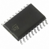
ST7FLIT19BF1M6 STMicroelectronics, ST7FLIT19BF1M6 Datasheet - Page 65

ST7FLIT19BF1M6
Manufacturer Part Number
ST7FLIT19BF1M6
Description
IC MCU 8BIT 4K FLASH 20SOIC
Manufacturer
STMicroelectronics
Series
ST7r
Datasheet
1.ST7FLIT15BY1M6.pdf
(159 pages)
Specifications of ST7FLIT19BF1M6
Core Processor
ST7
Core Size
8-Bit
Speed
8MHz
Connectivity
SPI
Peripherals
LVD, POR, PWM, WDT
Number Of I /o
17
Program Memory Size
4KB (4K x 8)
Program Memory Type
FLASH
Eeprom Size
128 x 8
Ram Size
256 x 8
Voltage - Supply (vcc/vdd)
2.7 V ~ 5.5 V
Data Converters
A/D 7x10b
Oscillator Type
Internal
Operating Temperature
-40°C ~ 85°C
Package / Case
20-SOIC (7.5mm Width)
Processor Series
ST7FLIT1x
Core
ST7
Data Bus Width
8 bit
Data Ram Size
256 B
Interface Type
SPI
Maximum Clock Frequency
8 MHz
Number Of Programmable I/os
17
Number Of Timers
4
Operating Supply Voltage
2.7 V to 5.5 V
Maximum Operating Temperature
+ 85 C
Mounting Style
SMD/SMT
Development Tools By Supplier
ST7FLITE-SK/RAIS, ST7FLIT1B-D/RAIS, ST7MDT10-DVP3, ST7MDT10-EMU3, STX-RLINK
Minimum Operating Temperature
- 40 C
On-chip Adc
10 bit, 7 Channel
For Use With
497-6232 - BOARD EVAL ST7LITE1B,STP5NK60Z497-5049 - KIT STARTER RAISONANCE ST7FLITE497-5046 - KIT TOOL FOR ST7/UPSD/STR7 MCU
Lead Free Status / RoHS Status
Lead free / RoHS Compliant
Other names
497-5627-5
- Current page: 65 of 159
- Download datasheet (3Mb)
DUAL 12-BIT AUTORELOAD TIMER 4 (Cont’d)
■
Pulses that last more than 8μs can be measured
with an accuracy of 4μs if f
lowing conditions:
– The 12-bit AT4 Timer is clocked by the Lite Timer
– The ICS bit in the ATCSR2 register is set so that
Figure 45. Long Range Input Capture Block Diagram
Notes:
1. Since the input capture flags (ICF) for both tim-
ers (AT4 Timer and LT Timer) are set when signal
transition occurs, software must mask one inter-
rupt by clearing the corresponding ICIE bit before
setting the ICS bit.
2. If the ICS bit changes (from 0 to 1 or from 1 to
0), a spurious transition might occur on the input
capture signal because of different values on LTIC
and ATIC. To avoid this situation, it is recommend-
ed to do as follows:
– First, reset both ICIE bits.
– Then set the ICS bit.
– Reset both ICF bits.
ATIC
LTIC
(RTC pulse: CK[1:0] = 01 in the ATCSR register)
the LTIC pin is used to trigger the AT4 Timer cap-
ture.
Long Input Capture
ICS
1
0
f
LTIMER
32MHz
OFF
f
cpu
f
OSC/32
OSC
LTICR
= 8 MHz in the fol-
CNTR1
ATR1
ATICR
12-bit Input Capture Register
8-bit Input Capture Register
12-bit AutoReload Register
8-bit Timebase Counter1
12-bit Upcounter1
– The signal to be captured is connected to LTIC
– Input Capture registers LTICR, ATICRH and
This configuration allows to cascade the Lite Timer
and the 12-bit AT4 Timer to get a 20-bit input cap-
ture value. Refer to
– And then set the ICIE bit of desired interrupt.
3. How to compute a pulse length with long input
capture feature.
As both timers are used, computing a pulse length
is not straight-forward. The procedure is as fol-
lows:
– At the first input capture on the rising edge of the
Refer to
pin
ATICRL are read
pulse, we assume that values in the registers are
as follows:
LTICR = LT1
ATICRH = ATH1
ATICRL = ATL1
Hence ATICR1 [11:0] = ATH1 & ATL1
12-Bit ARTIMER
LITE TIMER
Figure
12.
Figure
8 LSB bits
12 MSB bits
11.
ST7LITE1xB
20
cascaded
bits
65/159
1
Related parts for ST7FLIT19BF1M6
Image
Part Number
Description
Manufacturer
Datasheet
Request
R

Part Number:
Description:
STMicroelectronics [RIPPLE-CARRY BINARY COUNTER/DIVIDERS]
Manufacturer:
STMicroelectronics
Datasheet:

Part Number:
Description:
STMicroelectronics [LIQUID-CRYSTAL DISPLAY DRIVERS]
Manufacturer:
STMicroelectronics
Datasheet:

Part Number:
Description:
BOARD EVAL FOR MEMS SENSORS
Manufacturer:
STMicroelectronics
Datasheet:

Part Number:
Description:
NPN TRANSISTOR POWER MODULE
Manufacturer:
STMicroelectronics
Datasheet:

Part Number:
Description:
TURBOSWITCH ULTRA-FAST HIGH VOLTAGE DIODE
Manufacturer:
STMicroelectronics
Datasheet:

Part Number:
Description:
Manufacturer:
STMicroelectronics
Datasheet:

Part Number:
Description:
DIODE / SCR MODULE
Manufacturer:
STMicroelectronics
Datasheet:

Part Number:
Description:
DIODE / SCR MODULE
Manufacturer:
STMicroelectronics
Datasheet:

Part Number:
Description:
Search -----> STE16N100
Manufacturer:
STMicroelectronics
Datasheet:

Part Number:
Description:
Search ---> STE53NA50
Manufacturer:
STMicroelectronics
Datasheet:

Part Number:
Description:
NPN Transistor Power Module
Manufacturer:
STMicroelectronics
Datasheet:

Part Number:
Description:
DIODE / SCR MODULE
Manufacturer:
STMicroelectronics
Datasheet:


