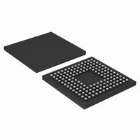
LPC2292FET144/01,5 NXP Semiconductors, LPC2292FET144/01,5 Datasheet - Page 18

LPC2292FET144/01,5
Manufacturer Part Number
LPC2292FET144/01,5
Description
IC ARM7 MCU FLASH 256K 144TFBGA
Manufacturer
NXP Semiconductors
Series
LPC2200r
Datasheet
1.LPC2292FBD144015.pdf
(53 pages)
Specifications of LPC2292FET144/01,5
Core Processor
ARM7
Core Size
16/32-Bit
Speed
60MHz
Connectivity
CAN, EBI/EMI, I²C, Microwire, SPI, SSI, SSP, UART/USART
Peripherals
POR, PWM, WDT
Number Of I /o
112
Program Memory Size
256KB (256K x 8)
Program Memory Type
FLASH
Ram Size
16K x 8
Voltage - Supply (vcc/vdd)
1.65 V ~ 3.6 V
Data Converters
A/D 8x10b
Oscillator Type
Internal
Operating Temperature
-40°C ~ 85°C
Package / Case
144-TFBGA
Processor Series
LPC22
Core
ARM7TDMI-S
Data Bus Width
32 bit
Data Ram Size
16 KB
Interface Type
CAN, I2C, JTAG, SPI, SSP, UART
Maximum Clock Frequency
60 MHz
Number Of Programmable I/os
112
Number Of Timers
2
Operating Supply Voltage
3.3 V
Maximum Operating Temperature
+ 85 C
Mounting Style
SMD/SMT
3rd Party Development Tools
MDK-ARM, RL-ARM, ULINK2
Minimum Operating Temperature
- 40 C
On-chip Adc
10 bit, 8 Channel
Package
144TFBGA
Device Core
ARM7TDMI-S
Family Name
LPC2000
Maximum Speed
60 MHz
For Use With
OM10091 - KIT DEV PHYCORE-ARM7/LPC2220622-1005 - USB IN-CIRCUIT PROG ARM7 LPC2K568-1757 - BOARD EVAL FOR LPC220X ARM MCU
Lead Free Status / RoHS Status
Lead free / RoHS Compliant
Eeprom Size
-
Lead Free Status / Rohs Status
Details
Other names
568-4320
935284897551
LPC2292FET144/01-S
LPC2292FET144/01-S
935284897551
LPC2292FET144/01-S
LPC2292FET144/01-S
Available stocks
Company
Part Number
Manufacturer
Quantity
Price
Company:
Part Number:
LPC2292FET144/01,5
Manufacturer:
NXP Semiconductors
Quantity:
10 000
NXP Semiconductors
LPC2292_2294_7
Product data sheet
6.6 Pin connect block
6.7 External memory controller
Table 5.
[1]
The pin connect block allows selected pins of the microcontroller to have more than one
function. Configuration registers control the multiplexers to allow connection between the
pin and the on chip peripherals. Peripherals should be connected to the appropriate pins
prior to being activated, and prior to any related interrupt(s) being enabled. Activity of any
enabled peripheral function that is not mapped to a related pin should be considered
undefined.
The external Static Memory Controller is a module which provides an interface between
the system bus and external (off-chip) memory devices. It provides support for up to four
independently configurable memory banks (16 MB each with byte lane enable control)
simultaneously. Each memory bank is capable of supporting SRAM, ROM, flash EPROM,
burst ROM memory, or some external I/O devices.
Each memory bank may be 8-bit, 16-bit, or 32-bit wide.
Block
UART1
PWM0
I2C
SPI0
SPI1 and SSP
PLL
RTC
System Control
ADC
CAN
SSP interface and UART0/1 auto-baud control are available on LPC2292/2294/01 only.
Interrupt sources
[1]
Flag(s)
RX Line Status (RLS)
Transmit Holding Register empty (THRE)
RX Data Available (RDA)
Character Time-out Indicator (CTI)
Modem Status Interrupt (MSI)
Auto-baud time-out (ABTO)
End of auto-baud (ABEO)
Match 0 to 6 (MR0, MR1, MR2, MR3, MR4, MR5, MR6)
SI (state change)
SPIF, MODF
SPIF, MODF and TXRIS, RXRIS, RTRIS, RORRIS
PLL Lock (PLOCK)
RTCCIF (Counter Increment), RTCALF (Alarm)
External Interrupt 0 (EINT0)
External Interrupt 1 (EINT1)
External Interrupt 2 (EINT2)
External Interrupt 3 (EINT3)
ADC
1 ORed CAN Acceptance Filter
CAN1/2 Tx
CAN2/3 Tx (LPC2294 only)
reserved
CAN1/2 Rx
CAN3/4 Rx (LPC2294 only)
Rev. 7 — 4 December 2008
16/32-bit ARM microcontrollers with external memory interface
…continued
[1]
[1]
LPC2292/LPC2294
© NXP B.V. 2008. All rights reserved.
VIC channel #
7
8
9
10
11
12
13
14
15
16
17
18
19
20, 21
22, 23
24, 25
26, 27
28,29
18 of 53


