LPC2292FET144/01,5 NXP Semiconductors, LPC2292FET144/01,5 Datasheet - Page 15
LPC2292FET144/01,5
Manufacturer Part Number
LPC2292FET144/01,5
Description
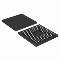
IC ARM7 MCU FLASH 256K 144TFBGA
Manufacturer
NXP Semiconductors
Series
LPC2200r
Datasheet
1.LPC2292FBD144015.pdf
(53 pages)
Specifications of LPC2292FET144/01,5
Core Processor
ARM7
Core Size
16/32-Bit
Speed
60MHz
Connectivity
CAN, EBI/EMI, I²C, Microwire, SPI, SSI, SSP, UART/USART
Peripherals
POR, PWM, WDT
Number Of I /o
112
Program Memory Size
256KB (256K x 8)
Program Memory Type
FLASH
Ram Size
16K x 8
Voltage - Supply (vcc/vdd)
1.65 V ~ 3.6 V
Data Converters
A/D 8x10b
Oscillator Type
Internal
Operating Temperature
-40°C ~ 85°C
Package / Case
144-TFBGA
Processor Series
LPC22
Core
ARM7TDMI-S
Data Bus Width
32 bit
Data Ram Size
16 KB
Interface Type
CAN, I2C, JTAG, SPI, SSP, UART
Maximum Clock Frequency
60 MHz
Number Of Programmable I/os
112
Number Of Timers
2
Operating Supply Voltage
3.3 V
Maximum Operating Temperature
+ 85 C
Mounting Style
SMD/SMT
3rd Party Development Tools
MDK-ARM, RL-ARM, ULINK2
Minimum Operating Temperature
- 40 C
On-chip Adc
10 bit, 8 Channel
Package
144TFBGA
Device Core
ARM7TDMI-S
Family Name
LPC2000
Maximum Speed
60 MHz
For Use With
OM10091 - KIT DEV PHYCORE-ARM7/LPC2220622-1005 - USB IN-CIRCUIT PROG ARM7 LPC2K568-1757 - BOARD EVAL FOR LPC220X ARM MCU
Lead Free Status / RoHS Status
Lead free / RoHS Compliant
Eeprom Size
-
Lead Free Status / Rohs Status
Details
Other names
568-4320
935284897551
LPC2292FET144/01-S
LPC2292FET144/01-S
935284897551
LPC2292FET144/01-S
LPC2292FET144/01-S
Available stocks
Company
Part Number
Manufacturer
Quantity
Price
Company:

Part Number:
LPC2292FET144/01,5
Manufacturer:
NXP Semiconductors
Quantity:
10 000


NXP Semiconductors
6. Functional description
LPC2292_2294_7
Product data sheet
6.1 Architectural overview
6.2 On-chip flash program memory
The ARM7TDMI-S is a general purpose 32-bit microprocessor, which offers high
performance and very low power consumption. The ARM architecture is based on RISC
principles, and the instruction set and related decode mechanism are much simpler than
those of microprogrammed CISC. This simplicity results in a high instruction throughput
and impressive real-time interrupt response from a small and cost-effective processor
core.
Pipeline techniques are employed so that all parts of the processing and memory systems
can operate continuously. Typically, while one instruction is being executed, its successor
is being decoded, and a third instruction is being fetched from memory.
The ARM7TDMI-S processor also employs a unique architectural strategy known as
Thumb, which makes it ideally suited to high-volume applications with memory
restrictions, or applications where code density is an issue.
The key idea behind Thumb is that of a super-reduced instruction set. Essentially, the
ARM7TDMI-S processor has two instruction sets:
The Thumb set’s 16-bit instruction length allows it to approach twice the density of
standard ARM code while retaining most of the ARM’s performance advantage over a
traditional 16-bit processor using 16-bit registers. This is possible because Thumb code
operates on the same 32-bit register set as ARM code.
Thumb code is able to provide up to 65 % of the code size of ARM, and 160 % of the
performance of an equivalent ARM processor connected to a 16-bit memory system.
The LPC2292/LPC2294 incorporate a 256 kB flash memory system respectively. This
memory may be used for both code and data storage. Programming of the flash memory
may be accomplished in several ways. It may be programmed In System via the serial
port. The application program may also erase and/or program the flash while the
application is running, allowing a great degree of flexibility for data storage field firmware
upgrades, etc. When the on-chip bootloader is used, 248 kB of flash memory is available
for user code.
The LPC2292/LPC2294 flash memory provides a minimum of 100000 erase/write cycles
and 20 years of data retention.
On-chip bootloader (as of revision 1.64) provides Code Read Protection (CRP) for the
LPC2292/LPC2294 on-chip flash memory. When the CRP is enabled, the JTAG debug
port, external memory boot and ISP commands accessing either the on-chip RAM or flash
memory are disabled. However, the ISP flash erase command can be executed at any
time (no matter whether the CRP is on or off). Removal of CRP is achieved by erasure of
full on-chip user flash. With the CRP off, full access to the chip via the JTAG and/or ISP is
restored.
•
•
The standard 32-bit ARM set
A 16-bit Thumb set
Rev. 7 — 4 December 2008
16/32-bit ARM microcontrollers with external memory interface
LPC2292/LPC2294
© NXP B.V. 2008. All rights reserved.
15 of 53
Related parts for LPC2292FET144/01,5
Image
Part Number
Description
Manufacturer
Datasheet
Request
R

Part Number:
Description:
NXP Semiconductors designed the LPC2420/2460 microcontroller around a 16-bit/32-bitARM7TDMI-S CPU core with real-time debug interfaces that include both JTAG andembedded trace
Manufacturer:
NXP Semiconductors
Datasheet:

Part Number:
Description:
NXP Semiconductors designed the LPC2458 microcontroller around a 16-bit/32-bitARM7TDMI-S CPU core with real-time debug interfaces that include both JTAG andembedded trace
Manufacturer:
NXP Semiconductors
Datasheet:
Part Number:
Description:
NXP Semiconductors designed the LPC2468 microcontroller around a 16-bit/32-bitARM7TDMI-S CPU core with real-time debug interfaces that include both JTAG andembedded trace
Manufacturer:
NXP Semiconductors
Datasheet:
Part Number:
Description:
NXP Semiconductors designed the LPC2470 microcontroller, powered by theARM7TDMI-S core, to be a highly integrated microcontroller for a wide range ofapplications that require advanced communications and high quality graphic displays
Manufacturer:
NXP Semiconductors
Datasheet:
Part Number:
Description:
NXP Semiconductors designed the LPC2478 microcontroller, powered by theARM7TDMI-S core, to be a highly integrated microcontroller for a wide range ofapplications that require advanced communications and high quality graphic displays
Manufacturer:
NXP Semiconductors
Datasheet:
Part Number:
Description:
The Philips Semiconductors XA (eXtended Architecture) family of 16-bit single-chip microcontrollers is powerful enough to easily handle the requirements of high performance embedded applications, yet inexpensive enough to compete in the market for hi
Manufacturer:
NXP Semiconductors
Datasheet:
Part Number:
Description:
The XA-S3 device is a member of Philips Semiconductors? XA(eXtended Architecture) family of high performance 16-bitsingle-chip microcontrollers
Manufacturer:
NXP Semiconductors
Datasheet:

Part Number:
Description:
The NXP BlueStreak LH75401/LH75411 family consists of two low-cost 16/32-bit System-on-Chip (SoC) devices
Manufacturer:
NXP Semiconductors
Datasheet:
Part Number:
Description:
The NXP LPC3130/3131 combine an 180 MHz ARM926EJ-S CPU core, high-speed USB2
Manufacturer:
NXP Semiconductors
Datasheet:
Part Number:
Description:
The NXP LPC3141 combine a 270 MHz ARM926EJ-S CPU core, High-speed USB 2
Manufacturer:
NXP Semiconductors
Part Number:
Description:
The NXP LPC3143 combine a 270 MHz ARM926EJ-S CPU core, High-speed USB 2
Manufacturer:
NXP Semiconductors

Part Number:
Description:
The NXP LPC3152 combines an 180 MHz ARM926EJ-S CPU core, High-speed USB 2
Manufacturer:
NXP Semiconductors
Part Number:
Description:
The NXP LPC3154 combines an 180 MHz ARM926EJ-S CPU core, High-speed USB 2
Manufacturer:
NXP Semiconductors

Part Number:
Description:
Standard level N-channel enhancement mode Field-Effect Transistor (FET) in a plastic package using NXP High-Performance Automotive (HPA) TrenchMOS technology
Manufacturer:
NXP Semiconductors
Datasheet: