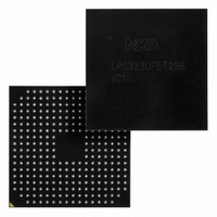
LPC3230FET296/01,5 NXP Semiconductors, LPC3230FET296/01,5 Datasheet - Page 8

LPC3230FET296/01,5
Manufacturer Part Number
LPC3230FET296/01,5
Description
IC ARM9 MCU 256K 296-TFBGA
Manufacturer
NXP Semiconductors
Series
LPC32x0r
Specifications of LPC3230FET296/01,5
Package / Case
296-TFBGA
Core Processor
ARM9
Core Size
16/32-Bit
Speed
266MHz
Connectivity
EBI/EMI, I²C, IrDA, Microwire, SPI, SSI, SSP, UART/USART, USB OTG
Peripherals
DMA, I²S, LCD, Motor Control PWM, PWM, WDT
Number Of I /o
51
Program Memory Type
ROMless
Ram Size
256K x 8
Voltage - Supply (vcc/vdd)
0.9 V ~ 3.6 V
Data Converters
A/D 3x10b
Oscillator Type
Internal
Operating Temperature
-40°C ~ 85°C
Processor Series
LPC32
Core
ARM926EJ-S
Data Bus Width
32 bit
Data Ram Size
256 KB
Interface Type
EMC
Maximum Clock Frequency
266 MHz
Number Of Timers
6
Operating Supply Voltage
1.31 V to 1.39 V
Maximum Operating Temperature
+ 85 C
Mounting Style
SMD/SMT
3rd Party Development Tools
MDK-ARM, RL-ARM, ULINK2
Minimum Operating Temperature
- 40 C
On-chip Adc
10 bit, 3 Channel
Lead Free Status / RoHS Status
Lead free / RoHS Compliant
Eeprom Size
-
Program Memory Size
-
Lead Free Status / Rohs Status
Lead free / RoHS Compliant
Other names
568-4964
935290764551
935290764551
Available stocks
Company
Part Number
Manufacturer
Quantity
Price
Company:
Part Number:
LPC3230FET296/01,5
Manufacturer:
NXP Semiconductors
Quantity:
10 000
NXP Semiconductors
ES_LPC3230
Errata sheet
Fig 3.
Fig 4.
128 MB DDR SDRAM example
Basic DDR write timing
EMC_DQM[1:0]
EMC_DQS[1:0]
3.3 DDR.2: DDR EMC_D[15:0] to EMC_DQS[1:0] data output set-up time,
EMC_D[15:0],
EMC_CLK
command
t
Remark: This affects both 1.8 V mobile and 2.5 V DDR SDRAM system implementations.
Introduction:
DDR memory interface signal EMC_DQS[1:0] is source synchronous, defined to be driven
by the MCU center aligned to the data EMC_D[15:0] for writes, while driven by the DDR
memory edge aligned to the EMC_D[15:0] for reads. The basic DDR write timing is shown
in the data sheet Fig 1.
Problem:
For DDR writes the LPC3230 drives the EMC_DQS[1:0] earlier in the data valid window
than center aligned. With the EMC_CLK at 133 MHz this produces a minimum set-up time
between the EMC_D[15:0] and EMC_DQS[1:0] of 600 ps across silicon process, voltage
and temperature. Test conditions are with the EMC buffers set to fast slew rate driving
su(Q)
, for MCU write to DDR provides limited timing margin
WRITE
All information provided in this document is subject to legal disclaimers.
t
DQSS
Rev. 8 — 1 February 2011
t
t
DQSL
DSS
t
su(Q)
t
h(Q)
t
t
DQSH
DSH
ES_LPC3230
Errata sheet LPC3230
002aae437
© NXP B.V. 2011. All rights reserved.
8 of 17


