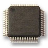
LPC11C14FBD48/301 NXP Semiconductors, LPC11C14FBD48/301 Datasheet - Page 25

LPC11C14FBD48/301
Manufacturer Part Number
LPC11C14FBD48/301
Description
IC MCU 32BIT 32KB FLASH 48LQFP
Manufacturer
NXP Semiconductors
Series
LPC1100r
Datasheets
1.LPC1114FHN333015.pdf
(66 pages)
2.LPC11C14FBD48301.pdf
(2 pages)
3.LPC11C14FBD48301.pdf
(61 pages)
Specifications of LPC11C14FBD48/301
Core Size
32-Bit
Program Memory Size
32KB (32K x 8)
Oscillator Type
Internal
Core Processor
ARM Cortex-M0
Speed
50MHz
Connectivity
CAN, I²C, Microwire, SPI, SSI, SSP, UART/USART
Peripherals
Brown-out Detect/Reset, POR, WDT
Number Of I /o
40
Program Memory Type
FLASH
Ram Size
8K x 8
Voltage - Supply (vcc/vdd)
1.8 V ~ 3.6 V
Data Converters
A/D 8x10b
Operating Temperature
-40°C ~ 85°C
Package / Case
48-LQFP
Controller Family/series
ARM Cortex-M0
No. Of I/o's
40
Ram Memory Size
8KB
Cpu Speed
50MHz
No. Of Timers
4
Processor Series
LPC11
Core
ARM Cortex M0
Data Bus Width
32 bit
Data Ram Size
8 KB
Interface Type
CAN, I2C, SPI, UART
Maximum Clock Frequency
50 MHz
Number Of Programmable I/os
40
Number Of Timers
1
Operating Supply Voltage
3.3 V
Maximum Operating Temperature
+ 85 C
Mounting Style
SMD/SMT
3rd Party Development Tools
MDK-ARM, RL-ARM, ULINK2
Minimum Operating Temperature
- 40 C
On-chip Adc
10 bit, 8 Channel
Lead Free Status / RoHS Status
Lead free / RoHS Compliant
Eeprom Size
-
Lead Free Status / Rohs Status
Details
Other names
568-5098
Available stocks
Company
Part Number
Manufacturer
Quantity
Price
Part Number:
LPC11C14FBD48/301
Manufacturer:
NXP/恩智浦
Quantity:
20 000
Company:
Part Number:
LPC11C14FBD48/301,
Manufacturer:
NXP Semiconductors
Quantity:
10 000
NXP Semiconductors
LPC11CX2_CX4
Product data sheet
7.16.5.2 Deep-sleep mode
7.16.5.3 Deep power-down mode
7.17.1 Start logic
7.17.2 Reset
7.17.3 Brownout detection
7.17 System control
In Deep-sleep mode, the chip is in Sleep mode, and in addition all analog blocks are shut
down. As an exception, the user has the option to keep the watchdog oscillator and the
BOD circuit running for self-timed wake-up and BOD protection. Deep-sleep mode allows
for additional power savings.
Up to 13 pins total, see
to wake up the chip from Deep-sleep mode.
Unless the watchdog oscillator is selected to run in Deep-sleep mode, the clock source
should be switched to IRC before entering Deep-sleep mode, because the IRC can be
switched on and off glitch-free.
In Deep power-down mode, power is shut off to the entire chip with the exception of the
WAKEUP pin. The LPC11Cx2/Cx4 can wake up from Deep power-down mode via the
WAKEUP pin.
When entering Deep power-down mode, an external pull-up resistor is required on the
WAKEUP pin to hold it HIGH. The RESET pin must also be held HIGH to prevent it from
floating while in Deep power-down mode.
The start logic connects external pins to corresponding interrupts in the NVIC. Each pin
shown in
vector table. The start logic pins can serve as external interrupt pins when the chip is
running. In addition, an input signal on the start logic pins can wake up the chip from
Deep-sleep mode when all clocks are shut down.
The start logic must be configured in the system configuration block and in the NVIC
before being used.
Reset has four sources on the LPC11Cx2/Cx4: the RESET pin, the Watchdog reset,
power-on reset (POR), and the BrownOut Detection (BOD) circuit. The RESET pin is a
Schmitt trigger input pin. Assertion of chip reset by any source, once the operating voltage
attains a usable level, starts the IRC and initializes the flash controller.
When the internal Reset is removed, the processor begins executing at address 0, which
is initially the Reset vector mapped from the boot block. At that point, all of the processor
and peripheral registers have been initialized to predetermined values.
An external pull-up resistor is required on the RESET pin if Deep power-down mode is
used.
The LPC11Cx2/Cx4 includes four levels for monitoring the voltage on the V
voltage falls below one of the four selected levels, the BOD asserts an interrupt signal to
the NVIC. This signal can be enabled for interrupt in the Interrupt Enable Register in the
Table 3
All information provided in this document is subject to legal disclaimers.
as input to the start logic has an individual interrupt in the NVIC interrupt
Rev. 2 — 3 December 2010
Table
3, serve as external wake-up pins to a dedicated start logic
32-bit ARM Cortex-M0 microcontroller
LPC11Cx2/Cx4
© NXP B.V. 2010. All rights reserved.
DD
pin. If this
25 of 61


