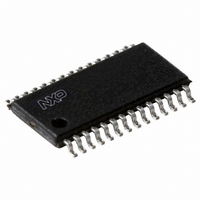
P89LPC932A1FDH,512 NXP Semiconductors, P89LPC932A1FDH,512 Datasheet - Page 31

P89LPC932A1FDH,512
Manufacturer Part Number
P89LPC932A1FDH,512
Description
IC 80C51 MCU FLASH 8K 28-TSSOP
Manufacturer
NXP Semiconductors
Series
LPC900r
Datasheet
1.P89LPC932A1FDH529.pdf
(64 pages)
Specifications of P89LPC932A1FDH,512
Program Memory Type
FLASH
Program Memory Size
8KB (8K x 8)
Package / Case
28-TSSOP
Core Processor
8051
Core Size
8-Bit
Speed
18MHz
Connectivity
I²C, SPI, UART/USART
Peripherals
Brown-out Detect/Reset, LED, POR, PWM, WDT
Number Of I /o
26
Ram Size
768 x 8
Voltage - Supply (vcc/vdd)
2.4 V ~ 3.6 V
Oscillator Type
Internal
Operating Temperature
-40°C ~ 85°C
Processor Series
P89LPC9x
Core
80C51
Data Bus Width
8 bit
Data Ram Size
768 B
Interface Type
I2C/SPI/UART
Maximum Clock Frequency
18 MHz
Number Of Programmable I/os
26
Number Of Timers
2
Operating Supply Voltage
2.4 V to 3.6 V
Maximum Operating Temperature
+ 85 C
Mounting Style
SMD/SMT
3rd Party Development Tools
PK51, CA51, A51, ULINK2
Minimum Operating Temperature
- 40 C
Cpu Family
89LP
Device Core
80C51
Device Core Size
8b
Frequency (max)
18MHz
Total Internal Ram Size
768Byte
# I/os (max)
26
Number Of Timers - General Purpose
2
Operating Supply Voltage (typ)
2.5/3.3V
Operating Supply Voltage (max)
3.6V
Operating Supply Voltage (min)
2.4V
Instruction Set Architecture
CISC
Operating Temp Range
-40C to 85C
Operating Temperature Classification
Industrial
Mounting
Surface Mount
Pin Count
28
Package Type
TSSOP
Lead Free Status / RoHS Status
Lead free / RoHS Compliant
For Use With
OM6292 - DEMO BOARD PCA2125 RTCDB-TSSOP-LPC932 - BOARD FOR LPC932 TSSOP622-1014 - BOARD FOR LPC9XX TSSOP622-1008 - BOARD FOR LPC9103 10-HVSON622-1006 - SOCKET ADAPTER BOARDMCB900K - BOARD PROTOTYPE NXP 89LPC9EPM900K - EMULATOR/PROGRAMMER NXP P89LPC9568-4000 - DEMO BOARD SPI/I2C TO DUAL UART568-3510 - DEMO BOARD SPI/I2C TO UART622-1003 - KIT FOR LCD DEMO622-1002 - USB IN-CIRCUIT PROG LPC9XX568-1759 - EMULATOR DEBUGGER/PROGRMMR LPC9X568-1758 - BOARD EVAL FOR LPC93X MCU FAMILY
Eeprom Size
-
Data Converters
-
Lead Free Status / Rohs Status
Lead free / RoHS Compliant
Other names
568-4515-5
935276132512
P89LPC932A1FDH
P89LPC932A1FDH
935276132512
P89LPC932A1FDH
P89LPC932A1FDH
NXP Semiconductors
P89LPC932A1_3
Product data sheet
7.20.3 Mode 2
7.20.4 Mode 3
7.20.5 Baud rate generator and selection
7.20.6 Framing error
7.20.7 Break detect
11 bits are transmitted (through TXD) or received (through RXD): start bit (logic 0), 8 data
bits (LSB first), a programmable 9
transmitted, the 9
Or, for example, the parity bit (P, in the PSW) could be moved into TB8. When data is
received, the 9
bit is not saved. The baud rate is programmable to either
frequency, as determined by the SMOD1 bit in PCON.
11 bits are transmitted (through TXD) or received (through RXD): a start bit (logic 0), 8
data bits (LSB first), a programmable 9
the same as Mode 2 in all respects except baud rate. The baud rate in Mode 3 is variable
and is determined by the Timer 1 overflow rate or the Baud Rate Generator (described in
Section 7.20.5 “Baud rate generator and
The P89LPC932A1 enhanced UART has an independent Baud Rate Generator. The baud
rate is determined by a baud-rate preprogrammed into the BRGR1 and BRGR0 SFRs
which together form a 16-bit baud rate divisor value that works in a similar manner as
Timer 1 but is much more accurate. If the baud rate generator is used, Timer 1 can be
used for other timing functions.
The UART can use either Timer 1 or the baud rate generator output (see
that Timer T1 is further divided by 2 if the SMOD1 bit (PCON.7) is cleared. The
independent Baud Rate Generator uses OSCCLK.
Framing error is reported in the status register (SSTAT). In addition, if SMOD0 (PCON.6)
is logic 1, framing errors can be made available in SCON.7 respectively. If SMOD0 is
logic 0, SCON.7 is SM0. It is recommended that SM0 and SM1 (SCON.7:6) are set up
when SMOD0 is logic 0.
Break detect is reported in the status register (SSTAT). A break is detected when
11 consecutive bits are sensed LOW. The break detect can be used to reset the device
and force the device into ISP mode.
Fig 13. Baud rate sources for UART (Modes 1, 3)
baud rate generator
timer 1 overflow
(CCLK-based)
(PCLK-based)
th
data bit goes into RB8 in Special Function Register SCON, while the stop
th
data bit (TB8 in SCON) can be assigned the value of logic 0 or logic 1.
Rev. 03 — 12 March 2007
8-bit microcontroller with accelerated two-clock 80C51 core
2
th
SMOD1 = 1
SMOD1 = 0
data bit, and a stop bit (logic 1). When data is
th
data bit, and a stop bit (logic 1). In fact, Mode 3 is
selection”).
SBRGS = 0
SBRGS = 1
1
16
P89LPC932A1
or
baud rate modes 1 and 3
1
32
of the CPU clock
© NXP B.V. 2007. All rights reserved.
Figure
002aaa897
13). Note
31 of 64


