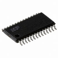
P89LPC932A1FDH,512 NXP Semiconductors, P89LPC932A1FDH,512 Datasheet - Page 29

P89LPC932A1FDH,512
Manufacturer Part Number
P89LPC932A1FDH,512
Description
IC 80C51 MCU FLASH 8K 28-TSSOP
Manufacturer
NXP Semiconductors
Series
LPC900r
Datasheet
1.P89LPC932A1FDH529.pdf
(64 pages)
Specifications of P89LPC932A1FDH,512
Program Memory Type
FLASH
Program Memory Size
8KB (8K x 8)
Package / Case
28-TSSOP
Core Processor
8051
Core Size
8-Bit
Speed
18MHz
Connectivity
I²C, SPI, UART/USART
Peripherals
Brown-out Detect/Reset, LED, POR, PWM, WDT
Number Of I /o
26
Ram Size
768 x 8
Voltage - Supply (vcc/vdd)
2.4 V ~ 3.6 V
Oscillator Type
Internal
Operating Temperature
-40°C ~ 85°C
Processor Series
P89LPC9x
Core
80C51
Data Bus Width
8 bit
Data Ram Size
768 B
Interface Type
I2C/SPI/UART
Maximum Clock Frequency
18 MHz
Number Of Programmable I/os
26
Number Of Timers
2
Operating Supply Voltage
2.4 V to 3.6 V
Maximum Operating Temperature
+ 85 C
Mounting Style
SMD/SMT
3rd Party Development Tools
PK51, CA51, A51, ULINK2
Minimum Operating Temperature
- 40 C
Cpu Family
89LP
Device Core
80C51
Device Core Size
8b
Frequency (max)
18MHz
Total Internal Ram Size
768Byte
# I/os (max)
26
Number Of Timers - General Purpose
2
Operating Supply Voltage (typ)
2.5/3.3V
Operating Supply Voltage (max)
3.6V
Operating Supply Voltage (min)
2.4V
Instruction Set Architecture
CISC
Operating Temp Range
-40C to 85C
Operating Temperature Classification
Industrial
Mounting
Surface Mount
Pin Count
28
Package Type
TSSOP
Lead Free Status / RoHS Status
Lead free / RoHS Compliant
For Use With
OM6292 - DEMO BOARD PCA2125 RTCDB-TSSOP-LPC932 - BOARD FOR LPC932 TSSOP622-1014 - BOARD FOR LPC9XX TSSOP622-1008 - BOARD FOR LPC9103 10-HVSON622-1006 - SOCKET ADAPTER BOARDMCB900K - BOARD PROTOTYPE NXP 89LPC9EPM900K - EMULATOR/PROGRAMMER NXP P89LPC9568-4000 - DEMO BOARD SPI/I2C TO DUAL UART568-3510 - DEMO BOARD SPI/I2C TO UART622-1003 - KIT FOR LCD DEMO622-1002 - USB IN-CIRCUIT PROG LPC9XX568-1759 - EMULATOR DEBUGGER/PROGRMMR LPC9X568-1758 - BOARD EVAL FOR LPC93X MCU FAMILY
Eeprom Size
-
Data Converters
-
Lead Free Status / Rohs Status
Lead free / RoHS Compliant
Other names
568-4515-5
935276132512
P89LPC932A1FDH
P89LPC932A1FDH
935276132512
P89LPC932A1FDH
P89LPC932A1FDH
NXP Semiconductors
P89LPC932A1_3
Product data sheet
7.19.7 Alternating output mode
7.19.8 PLL operation
In asymmetrical mode, the user can set up PWM channels A/B and C/D as alternating
pairs for bridge drive control. In this mode the output of these PWM channels are
alternately gated on every counter cycle.
The PWM module features a PLL that can be used to generate a CCUCLK frequency
between 16 MHz and 32 MHz. At this frequency the PWM module provides ultrasonic
PWM frequency with 10-bit resolution provided that the crystal frequency is 1 MHz or
higher. The PLL is fed an input signal from 0.5 MHz to 1 MHz and generates an output
signal of 32 times the input frequency. This signal is used to clock the timer. The user will
have to set a divider that scales PCLK by a factor from 1 to 16. This divider is found in the
SFR register TCR21. The PLL frequency can be expressed as shown in
Where: N is the value of PLLDV[3:0].
Since N ranges from 0 to 15, the CCLK frequency can be in the range of PCLK to
PLL frequency
Fig 11. Alternate output mode
=
----------------- -
PCLK
N
+
1
Rev. 03 — 12 March 2007
8-bit microcontroller with accelerated two-clock 80C51 core
002aaa895
TOR2
COMPARE VALUE A (or C)
COMPARE VALUE B (or D)
0
PWM OUTPUT (OCA or OCC)
PWM OUTPUT (OCB or OCD)
P89LPC932A1
TIMER VALUE
© NXP B.V. 2007. All rights reserved.
Equation
1.
PCLK
29 of 64
(1)
16
.


