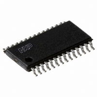
P89LPC936FDH,518 NXP Semiconductors, P89LPC936FDH,518 Datasheet - Page 30

P89LPC936FDH,518
Manufacturer Part Number
P89LPC936FDH,518
Description
IC 80C51 MCU FLASH 16K 28TSSOP
Manufacturer
NXP Semiconductors
Series
LPC900r
Datasheet
1.P89LPC936FDH518.pdf
(77 pages)
Specifications of P89LPC936FDH,518
Program Memory Type
FLASH
Program Memory Size
16KB (16K x 8)
Package / Case
28-TSSOP
Core Processor
8051
Core Size
8-Bit
Speed
18MHz
Connectivity
I²C, SPI, UART/USART
Peripherals
Brown-out Detect/Reset, LED, POR, PWM, WDT
Number Of I /o
26
Eeprom Size
512 x 8
Ram Size
768 x 8
Voltage - Supply (vcc/vdd)
2.4 V ~ 3.6 V
Data Converters
A/D 8x8b; D/A 2x8b
Oscillator Type
Internal
Operating Temperature
-40°C ~ 85°C
Processor Series
P89LPC9x
Core
80C51
Data Bus Width
8 bit
Data Ram Size
768 B
Interface Type
I2C/SPI/UART
Maximum Clock Frequency
18 MHz
Number Of Programmable I/os
26
Number Of Timers
2
Operating Supply Voltage
21 V
Maximum Operating Temperature
+ 85 C
Mounting Style
SMD/SMT
3rd Party Development Tools
PK51, CA51, A51, ULINK2
Minimum Operating Temperature
- 40 C
On-chip Adc
8-ch x 8-bit
On-chip Dac
2-ch x 8-bit
Lead Free Status / RoHS Status
Lead free / RoHS Compliant
For Use With
622-1014 - BOARD FOR LPC9XX TSSOP622-1008 - BOARD FOR LPC9103 10-HVSON622-1006 - SOCKET ADAPTER BOARDMCB900K - BOARD PROTOTYPE NXP 89LPC9EPM900K - EMULATOR/PROGRAMMER NXP P89LPC9568-4000 - DEMO BOARD SPI/I2C TO DUAL UART568-3510 - DEMO BOARD SPI/I2C TO UART622-1002 - USB IN-CIRCUIT PROG LPC9XX568-1759 - EMULATOR DEBUGGER/PROGRMMR LPC9X568-1758 - BOARD EVAL FOR LPC93X MCU FAMILY
Lead Free Status / Rohs Status
Lead free / RoHS Compliant
Other names
568-4339-2
935277841518
P89LPC936FDH-T
P89LPC936FDH-T
935277841518
P89LPC936FDH-T
P89LPC936FDH-T
NXP Semiconductors
P89LPC933_934_935_936
Product data sheet
8.13.1.1 Quasi-bidirectional output configuration
8.13.1.2 Open-drain output configuration
8.13.1 Port configurations
8.13 I/O ports
The P89LPC933/934/935/936 has four I/O ports: Port 0, Port 1, Port 2, and Port 3.
Ports 0, 1 and 2 are 8-bit ports, and Port 3 is a 2-bit port. The exact number of I/O pins
available depends upon the clock and reset options chosen, as shown in
Table 8.
[1]
All but three I/O port pins on the P89LPC933/934/935/936 may be configured by software
to one of four types on a bit-by-bit basis. These are: quasi-bidirectional (standard 80C51
port outputs), push-pull, open drain, and input-only. Two configuration registers for each
port select the output type for each port pin.
Quasi-bidirectional output type can be used as both an input and output without the need
to reconfigure the port. This is possible because when the port outputs a logic HIGH, it is
weakly driven, allowing an external device to pull the pin LOW. When the pin is driven
LOW, it is driven strongly and able to sink a fairly large current. These features are
somewhat similar to an open-drain output except that there are three pull-up transistors in
the quasi-bidirectional output that serve different purposes.
The P89LPC933/934/935/936 is a 3 V device, but the pins are 5 V-tolerant. In
quasi-bidirectional mode, if a user applies 5 V on the pin, there will be a current flowing
from the pin to V
quasi-bidirectional mode is discouraged.
A quasi-bidirectional port pin has a Schmitt trigger input that also has a glitch suppression
circuit.
The open-drain output configuration turns off all pull-ups and only drives the pull-down
transistor of the port driver when the port latch contains a logic 0. To be used as a logic
output, a port configured in this manner must have an external pull-up, typically a resistor
tied to V
Clock source
On-chip oscillator or watchdog
oscillator
External clock input
Low/medium/high speed oscillator
(external crystal or resonator)
1. P1.5 (RST) can only be an input and cannot be configured.
2. P1.2 (SCL/T0) and P1.3 (SDA/INT0) may only be configured to be either input-only or
Required for operation above 12 MHz.
open-drain.
DD
.
Number of I/O pins available
All information provided in this document is subject to legal disclaimers.
DD
, causing extra power consumption. Therefore, applying 5 V in
Rev. 8 — 12 January 2011
8-bit microcontroller with accelerated two-clock 80C51 core
Reset option
No external reset (except during
power-up)
External RST pin supported
No external reset (except during
power-up)
External RST pin supported
No external reset (except during
power-up)
External RST pin supported
P89LPC933/934/935/936
[1]
[1]
Number of I/O pins
(28-pin package)
26
25
25
24
24
23
© NXP B.V. 2011. All rights reserved.
Table
8.
30 of 77


