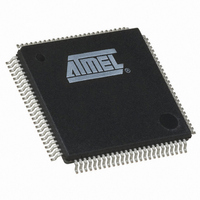
AT91SAM7A3-AU Atmel, AT91SAM7A3-AU Datasheet - Page 17

AT91SAM7A3-AU
Manufacturer Part Number
AT91SAM7A3-AU
Description
IC ARM7 MCU FLASH 256K 100LQFP
Manufacturer
Atmel
Series
AT91SAMr
Specifications of AT91SAM7A3-AU
Core Processor
ARM7
Core Size
16/32-Bit
Speed
60MHz
Connectivity
CAN, I²C, MMC, SPI, SSC, UART/USART
Peripherals
POR, PWM, WDT
Number Of I /o
62
Program Memory Size
256KB (256K x 8)
Program Memory Type
FLASH
Ram Size
32K x 8
Voltage - Supply (vcc/vdd)
1.65 V ~ 1.95 V
Data Converters
A/D 8x10b
Oscillator Type
Internal
Operating Temperature
-40°C ~ 85°C
Package / Case
100-LQFP
Controller Family/series
AT91SAM7xx
No. Of I/o's
62
Ram Memory Size
32KB
Cpu Speed
60MHz
No. Of Timers
3
Rohs Compliant
Yes
Package
100LQFP
Device Core
ARM7TDMI
Family Name
91S
Maximum Speed
60 MHz
Operating Supply Voltage
3.3 V
Data Bus Width
32 Bit
Number Of Programmable I/os
62
Interface Type
CAN/SPI/I2S/TWI/USART/USB
On-chip Adc
2(8-chx10-bit)
Number Of Timers
3
Processor Series
AT91SAMx
Core
ARM7TDMI
Data Ram Size
32 KB
Maximum Clock Frequency
60 MHz
Maximum Operating Temperature
+ 85 C
Mounting Style
SMD/SMT
3rd Party Development Tools
JTRACE-ARM-2M, MDK-ARM, RL-ARM, ULINK2
Development Tools By Supplier
AT91SAM-ICE, AT91-ISP, AT91SAM7A3-EK
Minimum Operating Temperature
- 40 C
Cpu Family
91S
Device Core Size
32b
Frequency (max)
60MHz
Total Internal Ram Size
32KB
# I/os (max)
62
Number Of Timers - General Purpose
3
Operating Supply Voltage (typ)
3.3V
Operating Supply Voltage (max)
3.6V
Operating Supply Voltage (min)
3V
Instruction Set Architecture
RISC
Operating Temp Range
-40C to 85C
Operating Temperature Classification
Industrial
Mounting
Surface Mount
Pin Count
100
Package Type
LQFP
For Use With
AT91SAM-ICE - EMULATOR FOR AT91 ARM7/ARM9AT91SAM7A3-EK - KIT EVAL FOR AT91SAM7A3
Lead Free Status / RoHS Status
Lead free / RoHS Compliant
Eeprom Size
-
Lead Free Status / Rohs Status
Details
Available stocks
Company
Part Number
Manufacturer
Quantity
Price
Company:
Part Number:
AT91SAM7A3-AU
Manufacturer:
MXIC
Quantity:
1 001
Company:
Part Number:
AT91SAM7A3-AU
Manufacturer:
Atmel
Quantity:
730
8.2
8.2.1
8.2.2
8.3
8.3.1
8.3.2
6042DS–ATARM–14-Dec-06
Memory Mapping
Embedded Flash
Internal SRAM
Internal Flash
Flash Overview
Embedded Flash Controller
The AT91SAM7A3 embeds a high-speed 32-Kbyte SRAM bank. After reset and until the Remap
Command is performed, the SRAM is only accessible at address 0x0020 0000. After Remap,
the SRAM also becomes available at address 0x0.
The AT91SAM7A3 features one bank of 256 Kbytes of Flash. The Flash is mapped to address
0x0010 0000. It is also accessible at address 0x0 after the reset and before the Remap
Command.
Figure 8-2.
The Flash block of the AT91SAM7A3 is organized in 1024 pages of 256 bytes. It reads as
65,536 32-bit words.
The Flash block contains a 256-byte write buffer, accessible through a 32-bit interface.
When Flash is not used (read or write access), it is automatically put into standby mode.
The Embedded Flash Controller (EFC) manages accesses performed by the masters of the sys-
tem. It enables reading the Flash and writing the write buffer. It also contains a User Interface
mapped within the Memory Controller on the APB. The User Interface allows:
• programming of the access parameters of the Flash (number of wait states, timings, etc.)
• starting commands such as full erase, page erase, page program, NVM bit set, NVM bit
• getting the end status of the last command
• getting error status
• programming interrupts on the end of the last commands or on errors
clear, etc.
256M Bytes
Internal Memory Mapping
0x0000 0000
0x0010 0000
0x0020 0000
0x0030 0000
0x000F FFFF
0x001F FFFF
0x002F FFFF
0x0FFF FFFF
Flash Before Remap
Undefined Areas
SRAM After Remap
Internal Flash
Internal SRAM
(Abort)
AT91SAM7A3
253M Bytes
1M Bytes
1M Bytes
1M Bytes
17


