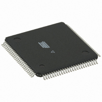
ATXMEGA64A1-AU Atmel, ATXMEGA64A1-AU Datasheet - Page 9

ATXMEGA64A1-AU
Manufacturer Part Number
ATXMEGA64A1-AU
Description
MCU AVR 64K FLASH 1.6V 100-TQFP
Manufacturer
Atmel
Series
AVR® XMEGAr
Datasheet
1.ATAVRONEKIT.pdf
(113 pages)
Specifications of ATXMEGA64A1-AU
Core Processor
AVR
Core Size
8/16-Bit
Speed
32MHz
Connectivity
EBI/EMI, I²C, IrDA, SPI, UART/USART
Peripherals
Brown-out Detect/Reset, DMA, POR, PWM, WDT
Number Of I /o
78
Program Memory Size
64KB (32K x 16)
Program Memory Type
FLASH
Eeprom Size
2K x 8
Ram Size
4K x 8
Voltage - Supply (vcc/vdd)
1.6 V ~ 3.6 V
Data Converters
A/D 16x12b, D/A 4x12b
Oscillator Type
Internal
Operating Temperature
-40°C ~ 85°C
Package / Case
100-TQFP, 100-VQFP
Processor Series
ATXMEGA64x
Core
AVR8
Data Bus Width
8 bit, 16 bit
Data Ram Size
4 KB
Interface Type
I2C/SPI/USART
Maximum Clock Frequency
32 MHz
Number Of Programmable I/os
78
Number Of Timers
8
Operating Supply Voltage
1.6 V to 3.6 V
Maximum Operating Temperature
+ 85 C
Mounting Style
SMD/SMT
3rd Party Development Tools
EWAVR, EWAVR-BL
Development Tools By Supplier
ATAVRDRAGON, ATAVRISP2, ATAVRONEKIT
Minimum Operating Temperature
- 40 C
On-chip Adc
2 (8-ch x 12-bit)
On-chip Dac
2 (2-ch x 12-bit)
Package
100TQFP
Device Core
AVR
Family Name
XMEGA
Maximum Speed
32 MHz
For Use With
ATAVRONEKIT - KIT AVR/AVR32 DEBUGGER/PROGRMMRATSTK600-TQFP100 - STK600 SOCKET/ADAPTER 100-TQFPATSTK600-TQFP44 - STK600 SOCKET/ADAPTER 44-TQFP770-1007 - ISP 4PORT ATMEL AVR MCU SPI/JTAG770-1004 - ISP 4PORT FOR ATMEL AVR MCU SPIATAVRISP2 - PROGRAMMER AVR IN SYSTEM
Lead Free Status / RoHS Status
Lead free / RoHS Compliant
Available stocks
Company
Part Number
Manufacturer
Quantity
Price
Company:
Part Number:
ATXMEGA64A1-AU
Manufacturer:
Atmel
Quantity:
135
6.3
6.4
6.5
8067M–AVR–09/10
Register File
ALU - Arithmetic Logic Unit
Program Flow
concept enables instructions to be executed in every clock cycle. The program memory is In-
System Self-Programmable Flash memory.
The fast-access Register File contains 32 x 8-bit general purpose working registers with single
clock cycle access time. This allows single-cycle Arithmetic Logic Unit (ALU) operation. In a typ-
ical ALU cycle, the operation is performed on two Register File operands, and the result is stored
back in the Register File.
Six of the 32 registers can be used as three 16-bit address register pointers for data space
addressing - enabling efficient address calculations. One of these address pointers can also be
used as an address pointer for look up tables in Flash program memory.
The high performance Arithmetic Logic Unit (ALU) supports arithmetic and logic operations
between registers or between a constant and a register. Single register operations can also be
executed. Within a single clock cycle, arithmetic operations between general purpose registers
or between a register and an immediate are executed. After an arithmetic or logic operation, the
Status Register is updated to reflect information about the result of the operation.
The ALU operations are divided into three main categories – arithmetic, logical, and bit-func-
tions. Both 8- and 16-bit arithmetic is supported, and the instruction set allows for efficient
implementation of 32-bit aritmetic. The ALU also provides a powerful multiplier supporting both
signed and unsigned multiplication and fractional format.
When the device is powered on, the CPU starts to execute instructions from the lowest address
in the Flash Program Memory ‘0’. The Program Counter (PC) addresses the next instruction to
be fetched. After a reset, the PC is set to location ‘0’.
Program flow is provided by conditional and unconditional jump and call instructions, capable of
addressing the whole address space directly. Most AVR instructions use a 16-bit word format,
while a limited number uses a 32-bit format.
During interrupts and subroutine calls, the return address PC is stored on the Stack. The Stack
is effectively allocated in the general data SRAM, and consequently the Stack size is only limited
by the total SRAM size and the usage of the SRAM. After reset the Stack Pointer (SP) points to
the highest address in the internal SRAM. The SP is read/write accessible in the I/O memory
space, enabling easy implementation of multiple stacks or stack areas. The data SRAM can
easily be accessed through the five different addressing modes supported in the AVR CPU.
XMEGA A1
9


