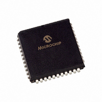
PIC16LF877A-I/L Microchip Technology, PIC16LF877A-I/L Datasheet - Page 137

PIC16LF877A-I/L
Manufacturer Part Number
PIC16LF877A-I/L
Description
IC MCU FLASH 8KX14 EE A/D 44PLCC
Manufacturer
Microchip Technology
Series
PIC® 16Fr
Specifications of PIC16LF877A-I/L
Core Size
8-Bit
Program Memory Size
14KB (8K x 14)
Core Processor
PIC
Speed
10MHz
Connectivity
I²C, SPI, UART/USART
Peripherals
Brown-out Detect/Reset, POR, PWM, WDT
Number Of I /o
33
Program Memory Type
FLASH
Eeprom Size
256 x 8
Ram Size
368 x 8
Voltage - Supply (vcc/vdd)
2 V ~ 5.5 V
Data Converters
A/D 8x10b
Oscillator Type
External
Operating Temperature
-40°C ~ 85°C
Package / Case
44-PLCC
Controller Family/series
PIC16LF
No. Of I/o's
33
Eeprom Memory Size
256Byte
Ram Memory Size
368Byte
Cpu Speed
20MHz
No. Of Timers
3
Lead Free Status / RoHS Status
Lead free / RoHS Compliant
Other names
PIC16LF877AI/L
Available stocks
Company
Part Number
Manufacturer
Quantity
Price
Company:
Part Number:
PIC16LF877A-I/L
Manufacturer:
Microchip Technology
Quantity:
10 000
- Current page: 137 of 234
- Download datasheet (5Mb)
12.0
The comparator module contains two analog compara-
tors. The inputs to the comparators are multiplexed
with I/O port pins RA0 through RA3, while the outputs
are multiplexed to pins RA4 and RA5. The on-chip volt-
age reference (Section 13.0 “Comparator Voltage
Reference Module”) can also be an input to the
comparators.
REGISTER 12-1:
2003 Microchip Technology Inc.
COMPARATOR MODULE
bit 7
bit 6
bit 5
bit 4
bit 3
bit 2
CMCON REGISTER
C2OUT: Comparator 2 Output bit
When C2INV = 0:
1 = C2 V
0 = C2 V
When C2INV = 1:
1 = C2 V
0 = C2 V
C1OUT: Comparator 1 Output bit
When C1INV = 0:
1 = C1 V
0 = C1 V
When C1INV = 1:
1 = C1 V
0 = C1 V
C2INV: Comparator 2 Output Inversion bit
1 = C2 output inverted
0 = C2 output not inverted
C1INV: Comparator 1 Output Inversion bit
1 = C1 output inverted
0 = C1 output not inverted
CIS: Comparator Input Switch bit
When CM2:CM0 = 110:
1 = C1 V
0 = C1 V
CM2:CM0: Comparator Mode bits
Figure 12-1 shows the Comparator modes and CM2:CM0 bit settings.
Legend:
R = Readable bit
- n = Value at POR
bit 7
C2OUT
R-0
C2 V
C2 V
IN
IN
IN
IN
IN
IN
IN
IN
IN
IN
IN
IN
+ > C2 V
+ < C2 V
+ < C2 V
+ > C2 V
+ > C1 V
+ < C1 V
+ < C1 V
+ > C1 V
- connects to RA3/AN3
- connects to RA2/AN2
- connects to RA0/AN0
- connects to RA1/AN1
C1OUT
R-0
IN
IN
IN
IN
IN
IN
IN
IN
-
-
-
-
-
-
-
-
C2INV
R/W-0
W = Writable bit
‘1’ = Bit is set
C1INV
R/W-0
The CMCON register (Register 12-1) controls the com-
parator input and output multiplexers. A block diagram
of the various comparator configurations is shown in
Figure 12-1.
R/W-0
U = Unimplemented bit, read as ‘0’
‘0’ = Bit is cleared
CIS
R/W-1
PIC16F87XA
CM2
x = Bit is unknown
R/W-1
CM1
DS39582B-page 135
R/W-1
CM0
bit 0
Related parts for PIC16LF877A-I/L
Image
Part Number
Description
Manufacturer
Datasheet
Request
R

Part Number:
Description:
IC MCU FLASH 4KX14 EEPROM 18SOIC
Manufacturer:
Microchip Technology
Datasheet:

Part Number:
Description:
IC MCU FLASH 4KX14 EEPROM 18DIP
Manufacturer:
Microchip Technology
Datasheet:

Part Number:
Description:
IC MCU FLASH 4KX14 EEPROM 20SSOP
Manufacturer:
Microchip Technology
Datasheet:

Part Number:
Description:
(PIC16LF87 / PIC16LF88) 18/20/28-Pin Enhanced FLASH Microcontrollers with nanoWatt Technology
Manufacturer:
Microchip Technology

Part Number:
Description:
IC MCU FLASH 4KX14 EEPROM 28QFN
Manufacturer:
Microchip Technology
Datasheet:

Part Number:
Description:
Manufacturer:
Microchip Technology Inc.
Datasheet:

Part Number:
Description:
Manufacturer:
Microchip Technology Inc.
Datasheet:

Part Number:
Description:
Manufacturer:
Microchip Technology Inc.
Datasheet:

Part Number:
Description:
Manufacturer:
Microchip Technology Inc.
Datasheet:

Part Number:
Description:
Manufacturer:
Microchip Technology Inc.
Datasheet:

Part Number:
Description:
Manufacturer:
Microchip Technology Inc.
Datasheet:


