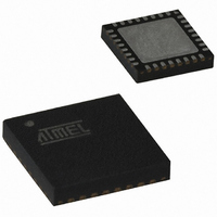
AT89C5130A-PUTUM Atmel, AT89C5130A-PUTUM Datasheet - Page 120

AT89C5130A-PUTUM
Manufacturer Part Number
AT89C5130A-PUTUM
Description
IC 8051 MCU FLASH 16K USB 32QFN
Manufacturer
Atmel
Series
AT89C513xr
Datasheet
1.AT89C5130A-PUTUM.pdf
(188 pages)
Specifications of AT89C5130A-PUTUM
Core Processor
C52X2
Core Size
8-Bit
Speed
48MHz
Connectivity
I²C, SPI, UART/USART, USB
Peripherals
LED, POR, PWM, WDT
Number Of I /o
18
Program Memory Size
16KB (16K x 8)
Program Memory Type
FLASH
Eeprom Size
4K x 8
Ram Size
1.25K x 8
Voltage - Supply (vcc/vdd)
2.7 V ~ 5.5 V
Oscillator Type
Internal
Operating Temperature
-40°C ~ 85°C
Package / Case
32-VQFN Exposed Pad, 32-HVQFN, 32-SQFN, 32-DHVQFN
Package
32QFN EP
Device Core
8051
Family Name
89C
Maximum Speed
48 MHz
Operating Supply Voltage
3.3|5 V
Data Bus Width
8 Bit
Number Of Programmable I/os
34
Interface Type
SPI/TWI/UART/USB
Number Of Timers
3
Processor Series
AT89x
Core
8051
Data Ram Size
1.25 KB
Maximum Clock Frequency
48 MHz
Maximum Operating Temperature
+ 85 C
Mounting Style
SMD/SMT
3rd Party Development Tools
PK51, CA51, A51, ULINK2
Development Tools By Supplier
AT89STK-05
Minimum Operating Temperature
- 40 C
Height
0.95 mm
Length
7 mm
Supply Voltage (max)
5.5 V
Supply Voltage (min)
2.7 V
Width
7 mm
For Use With
AT89OCD-01 - USB EMULATOR FOR AT8XC51 MCU
Lead Free Status / RoHS Status
Lead free / RoHS Compliant
Data Converters
-
Lead Free Status / Rohs Status
Details
Other names
AT89C5130A-PUTIM
AT89C5130A-PUTIM
AT89C5130A-PUTIM
Available stocks
Company
Part Number
Manufacturer
Quantity
Price
Company:
Part Number:
AT89C5130A-PUTUM
Manufacturer:
Atmel
Quantity:
5
21. USB Controller
21.1
Figure 21-1. USB Device Controller Block Diagram
21.1.1
120
Description
AT89C5130A/31A-M
Serial Interface Engine (SIE)
D+
D-
.
The USB device controller provides the hardware that the AT89C5131 needs to interface a USB
link to a data flow stored in a double port memory (DPRAM).
The USB controller requires a 48 MHz ±0.25% reference clock, which is the output of the
AT89C5131 PLL (see Section “PLL”, page 15) divided by a clock prescaler. This clock is used to
generate a 12 MHz Full-speed bit clock from the received USB differential data and to transmit
data according to full speed USB device tolerance. Clock recovery is done by a Digital Phase
Locked Loop (DPLL) block, which is compliant with the jitter specification of the USB bus.
The Serial Interface Engine (SIE) block performs NRZI encoding and decoding, bit stuffing, CRC
generation and checking, and the serial-parallel data conversion.
The Universal Function Interface (UFI) realizes the interface between the data flow and the Dual
Port RAM.
The SIE performs the following functions:
USB
D+/D-
Buffer
• NRZI data encoding and decoding.
• Bit stuffing and un-stuffing.
• CRC generation and checking.
• Handshakes.
• TOKEN type identifying.
DPLL
SIE
48 MHz
12 MHz
+/- 0.25%
UFI
C51
Microcontroller
Interface
Up to 48 MHz
UC_sysclk
4337K–USB–04/08


