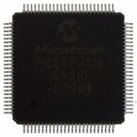
PIC24FJ128GA010-I/PT Microchip Technology, PIC24FJ128GA010-I/PT Datasheet - Page 3

PIC24FJ128GA010-I/PT
Manufacturer Part Number
PIC24FJ128GA010-I/PT
Description
IC PIC MCU FLASH 128K 100TQFP
Manufacturer
Microchip Technology
Series
PIC® 24Fr
Datasheets
1.PIC24FJ16GA002-ISS.pdf
(52 pages)
2.PIC24FJ64GA006-IPT.pdf
(240 pages)
3.PIC24FJ64GA006-IPT.pdf
(22 pages)
4.PIC24FJ128GA008-IPT.pdf
(12 pages)
5.PIC24FJ128GA006-IPT.pdf
(231 pages)
6.PIC24FJ128GA010-IPT.pdf
(230 pages)
Specifications of PIC24FJ128GA010-I/PT
Core Size
16-Bit
Program Memory Size
128KB (43K x 24)
Core Processor
PIC
Speed
16MHz
Connectivity
I²C, PMP, SPI, UART/USART
Peripherals
Brown-out Detect/Reset, POR, PWM, WDT
Number Of I /o
84
Program Memory Type
FLASH
Ram Size
8K x 8
Voltage - Supply (vcc/vdd)
2 V ~ 3.6 V
Data Converters
A/D 16x10b
Oscillator Type
Internal
Operating Temperature
-40°C ~ 85°C
Package / Case
100-TFQFP
Controller Family/series
PIC24
No. Of I/o's
84
Ram Memory Size
8KB
Cpu Speed
32MHz
No. Of Timers
5
No. Of Pwm Channels
5
Embedded Interface Type
EUART, I2C, PSP, SPI
Rohs Compliant
Yes
Processor Series
PIC24FJ
Core
PIC
Data Bus Width
16 bit
Data Ram Size
8 KB
Interface Type
SPI, I2C, USART
Maximum Clock Frequency
16 MHz
Number Of Programmable I/os
54
Number Of Timers
5
Maximum Operating Temperature
+ 85 C
Mounting Style
SMD/SMT
3rd Party Development Tools
52713-733, 52714-737, 53276-922, EWDSPIC
Development Tools By Supplier
PG164130, DV164035, DV244005, DV164005, PG164120, DM240001, DM240011
Minimum Operating Temperature
- 40 C
On-chip Adc
10 bit, 16 Channel
Package
100TQFP
Device Core
PIC
Family Name
PIC24
Maximum Speed
16 MHz
Operating Supply Voltage
2.5|3.3 V
Lead Free Status / RoHS Status
Lead free / RoHS Compliant
For Use With
DM240011 - KIT STARTER MPLAB FOR PIC24F MCUAC164333 - MODULE SKT FOR PM3 100QFPDV164033 - KIT START EXPLORER 16 MPLAB ICD2MA160011 - DAUGHTER BOARD PICDEM LCD 16F91XDM240001 - BOARD DEMO PIC24/DSPIC33/PIC32
Eeprom Size
-
Lead Free Status / Rohs Status
Details
Available stocks
Company
Part Number
Manufacturer
Quantity
Price
Company:
Part Number:
PIC24FJ128GA010-I/PT
Manufacturer:
Microchi
Quantity:
627
Company:
Part Number:
PIC24FJ128GA010-I/PT
Manufacturer:
MICROCHIP
Quantity:
212
Company:
Part Number:
PIC24FJ128GA010-I/PT
Manufacturer:
Microchip Technology
Quantity:
10 000
2.2
The Flash program memory on the PIC24FJXXXGA0XX
devices has a specific write/erase requirement that must
be adhered to for proper device operation. The rule is
that any given word in memory must not be written more
than twice before erasing the page in which it is located.
Thus, the easiest way to conform to this rule is to write
all the data in a programming block within one write
cycle. The programming methods specified in this
specification comply with this requirement.
TABLE 2-1:
© 2008 Microchip Technology Inc.
MCLR
ENVREG
DISVREG
V
V
V
PGC1
PGD1
PGC2
PGD2
Legend: I = Input, O = Output, P = Power
Note 1:
Note:
DD
SS
DDCORE
Pin Name
and AV
and AV
2:
Program Memory Write/Erase
Requirements
(1)
Applies to 28 and 44-pin devices only.
All power supply and ground pins must be connected, including analog supplies (AV
(AV
Writing to a location multiple times without
erasing is not recommended.
SS
DD
(2)
SS
(2)
).
PIN DESCRIPTIONS (DURING PROGRAMMING)
Pin Name
DISVREG
ENVREG
V
MCLR
DDCORE
PGC
PGD
PGC
PGD
V
V
DD
SS
Pin Type
I/O
I/O
P
P
P
P
I
I
I
I
Programming Enable
Enable for On-Chip Voltage Regulator
Disable for On-Chip Voltage Regulator
Power Supply
Ground
Regulated Power Supply for Core
Primary Programming Pin Pair: Serial Clock
Primary Programming Pin Pair: Serial Data
Secondary Programming Pin Pair: Serial Clock
Secondary Programming Pin Pair: Serial Data
During Programming
2.3
The pin diagrams for the PIC24FJXXXGA0XX family
are shown in the following figures. The pins that are
required for programming are listed in Table 2-1 and
are shown in bold letters in the figures. Refer to the
appropriate device data sheet for complete pin
descriptions.
PIC24FJXXXGA0XX
Pin Diagrams
Pin Description
DD
) and ground
DS39768D-page 3


