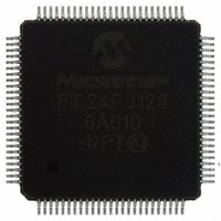
PIC24FJ128GA010-I/PT Microchip Technology, PIC24FJ128GA010-I/PT Datasheet - Page 21

PIC24FJ128GA010-I/PT
Manufacturer Part Number
PIC24FJ128GA010-I/PT
Description
IC PIC MCU FLASH 128K 100TQFP
Manufacturer
Microchip Technology
Series
PIC® 24Fr
Datasheets
1.PIC24FJ16GA002-ISS.pdf
(52 pages)
2.PIC24FJ64GA006-IPT.pdf
(240 pages)
3.PIC24FJ64GA006-IPT.pdf
(22 pages)
4.PIC24FJ128GA008-IPT.pdf
(12 pages)
5.PIC24FJ128GA006-IPT.pdf
(231 pages)
6.PIC24FJ128GA010-IPT.pdf
(230 pages)
Specifications of PIC24FJ128GA010-I/PT
Core Size
16-Bit
Program Memory Size
128KB (43K x 24)
Core Processor
PIC
Speed
16MHz
Connectivity
I²C, PMP, SPI, UART/USART
Peripherals
Brown-out Detect/Reset, POR, PWM, WDT
Number Of I /o
84
Program Memory Type
FLASH
Ram Size
8K x 8
Voltage - Supply (vcc/vdd)
2 V ~ 3.6 V
Data Converters
A/D 16x10b
Oscillator Type
Internal
Operating Temperature
-40°C ~ 85°C
Package / Case
100-TFQFP
Controller Family/series
PIC24
No. Of I/o's
84
Ram Memory Size
8KB
Cpu Speed
32MHz
No. Of Timers
5
No. Of Pwm Channels
5
Embedded Interface Type
EUART, I2C, PSP, SPI
Rohs Compliant
Yes
Processor Series
PIC24FJ
Core
PIC
Data Bus Width
16 bit
Data Ram Size
8 KB
Interface Type
SPI, I2C, USART
Maximum Clock Frequency
16 MHz
Number Of Programmable I/os
54
Number Of Timers
5
Maximum Operating Temperature
+ 85 C
Mounting Style
SMD/SMT
3rd Party Development Tools
52713-733, 52714-737, 53276-922, EWDSPIC
Development Tools By Supplier
PG164130, DV164035, DV244005, DV164005, PG164120, DM240001, DM240011
Minimum Operating Temperature
- 40 C
On-chip Adc
10 bit, 16 Channel
Package
100TQFP
Device Core
PIC
Family Name
PIC24
Maximum Speed
16 MHz
Operating Supply Voltage
2.5|3.3 V
Lead Free Status / RoHS Status
Lead free / RoHS Compliant
For Use With
DM240011 - KIT STARTER MPLAB FOR PIC24F MCUAC164333 - MODULE SKT FOR PM3 100QFPDV164033 - KIT START EXPLORER 16 MPLAB ICD2MA160011 - DAUGHTER BOARD PICDEM LCD 16F91XDM240001 - BOARD DEMO PIC24/DSPIC33/PIC32
Eeprom Size
-
Lead Free Status / Rohs Status
Details
Available stocks
Company
Part Number
Manufacturer
Quantity
Price
Company:
Part Number:
PIC24FJ128GA010-I/PT
Manufacturer:
Microchi
Quantity:
627
Company:
Part Number:
PIC24FJ128GA010-I/PT
Manufacturer:
MICROCHIP
Quantity:
212
Company:
Part Number:
PIC24FJ128GA010-I/PT
Manufacturer:
Microchip Technology
Quantity:
10 000
3.7
The PIC24FJXXXGA0XX family configuration is stored
in Flash Configuration Words at the end of the user
space program memory and in multiple register
Configuration Words located in the test space.
These registers reflect values read at any Reset from
program memory locations. The values can be changed
only by programming the content of the corresponding
Flash Configuration Word and resetting the device. The
Reset forces an automatic reload of the Flash stored
configuration values by sequencing through the
dedicated Flash Configuration Words and transferring
the data into the Configuration registers. To change the
values of the Flash Configuration Word once it has been
programmed, the device must be Chip Erased, as
described in Section 3.5 “Erasing Program Memory”,
and reprogrammed to the desired value. It is not
possible to program a ‘0’ to ‘1’, but they may be
programmed from a ‘1’ to ‘0’ to enable code protection.
Table 3-7 shows the ICSP programming details for pro-
gramming the Configuration Word locations, including
the serial pattern with the ICSP command code which
must be transmitted, Least Significant bit first, using the
PGCx and PGDx pins (see Figure 3-2).
© 2008 Microchip Technology Inc.
Writing Configuration Words
In Step 1, the Reset vector is exited. In Step 2, the
NVMCON register is initialized for programming of
code memory. In Step 3, the 24-bit starting destination
address for programming is loaded into the TBLPAG
register and W7 register.
The TBLPAG register must be loaded with the
following:
• 96 and 64 Kbyte devices – 00h
• 128 Kbyte devices – 01h
To verify the data by reading the Configuration Words
after performing the write in order, the code protection
bits initially should be programmed to a ‘1’ to ensure
that the verification can be performed properly. After
verification is finished, the code protection bit can be
programmed to a ‘0’ by using a word write to the
appropriate Configuration Word.
TABLE 3-6:
Last Word
Last Word – 2
Note 1:
PIC24FJXXXGA0XX
Address
CW1<15> is reserved and must be
programmed to ‘0’.
DEFAULT CONFIGURATION
REGISTER VALUES
Name
CW1
CW2
DS39768D-page 21
Default Value
7FFFh
FFFFh
(1)


