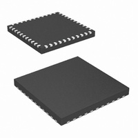
PIC18F47J13-I/ML Microchip Technology, PIC18F47J13-I/ML Datasheet - Page 382

PIC18F47J13-I/ML
Manufacturer Part Number
PIC18F47J13-I/ML
Description
IC PIC MCU 128KB FLASH 44QFN
Manufacturer
Microchip Technology
Series
PIC® XLP™ 18Fr
Datasheets
1.PIC18LF24J10-ISS.pdf
(32 pages)
2.PIC18F26J13-ISS.pdf
(496 pages)
3.PIC18F26J13-ISS.pdf
(558 pages)
4.PIC18F26J13-ISS.pdf
(12 pages)
Specifications of PIC18F47J13-I/ML
Core Size
8-Bit
Program Memory Size
128KB (64K x 16)
Core Processor
PIC
Speed
48MHz
Connectivity
I²C, LIN, SPI, UART/USART
Peripherals
Brown-out Detect/Reset, POR, PWM, WDT
Number Of I /o
34
Program Memory Type
FLASH
Ram Size
3.8K x 8
Voltage - Supply (vcc/vdd)
2.15 V ~ 3.6 V
Data Converters
A/D 13x10b/12b
Oscillator Type
Internal
Operating Temperature
-40°C ~ 85°C
Package / Case
*
Controller Family/series
PIC18
Cpu Speed
48MHz
Digital Ic Case Style
QFN
Supply Voltage Range
1.8V To 5.5V
Embedded Interface Type
I2C, SPI, USART
Rohs Compliant
Yes
Processor Series
PIC18F
Core
PIC
Data Bus Width
8 bit
Data Ram Size
4 KB
Interface Type
I2C, SPI, EUSART
Maximum Clock Frequency
48 MHz
Number Of Programmable I/os
25
Number Of Timers
8
Operating Supply Voltage
2 V to 3.6 V
Maximum Operating Temperature
+ 85 C
Mounting Style
SMD/SMT
3rd Party Development Tools
52715-96, 52716-328, 52717-734, 52712-325, EWPIC18
Development Tools By Supplier
DM164128, DM180021, DM183026-2, DV164131, MA180030, DM183022, DM183032, DV164136, MA180024
Minimum Operating Temperature
- 40 C
On-chip Adc
12 bit, 13 Channel
Lead Free Status / RoHS Status
Lead free / RoHS Compliant
For Use With
MA180030 - BOARD DEMO PIC18F47J13 FS USBMA180029 - BOARD DEMO PIC18F47J53 FS USB
Eeprom Size
-
Lead Free Status / Rohs Status
Details
- PIC18LF24J10-ISS PDF datasheet
- PIC18F26J13-ISS PDF datasheet #2
- PIC18F26J13-ISS PDF datasheet #3
- PIC18F26J13-ISS PDF datasheet #4
- Current page: 382 of 558
- Download datasheet (5Mb)
PIC18F47J13 FAMILY
23.2
A single comparator is shown in Figure 23-2, along with
the relationship between the analog input levels and
the digital output. When the analog input at V
than the analog input, V
tor is a digital low level. When the analog input at V
is greater than the analog input, V
comparator is a digital high level. The shaded areas of
the output of the comparator, in Figure 23-2, represent
the uncertainty due to input offsets and response time.
FIGURE 23-2:
FIGURE 23-3:
DS39974A-page 382
V
V
Output
IN
IN
-
+
V
V
IN
IN
Comparator Operation
+
-
VA
R
S
Legend:
+
–
< 10k
SINGLE COMPARATOR
COMPARATOR ANALOG INPUT MODEL
IN
-, the output of the compara-
A
IN
C
V
I
R
R
VA
LEAKAGE
C
5 pF
PIN
T
IC
S
IN
PIN
-, the output of the
Output
= Input Capacitance
= Threshold Voltage
= Leakage Current at the pin due to various junctions
= Interconnect Resistance
= Source Impedance
= Analog Voltage
IN
+ is less
Preliminary
IN
V
+
DD
V
V
T
T
= 0.6V
= 0.6V
23.3
Response time is the minimum time, after selecting a
new reference voltage or input source, before the
comparator output has a valid level. The response time
of the comparator differs from the settling time of the
voltage reference. Therefore, both of these times must
be considered when determining the total response to
a comparator input change. Otherwise, the maximum
delay of the comparators should be used (see
Section 30.0 “Electrical Characteristics”).
23.4
Figure 23-3 provides a simplified circuit for an analog
input. Since the analog pins are connected to a digital
output, they have reverse biased diodes to V
V
and V
by more than 0.6V in either direction, one of the diodes
is forward biased and a latch-up condition may occur.
A maximum source impedance of 10 k is
recommended for the analog sources. Any external
component connected to an analog input pin, such as
a capacitor or a Zener diode, should have very little
leakage current.
SS
. The analog input, therefore, must be between V
DD
. If the input voltage deviates from this range,
Comparator
Analog Input Connection
Considerations
I
±100 nA
V
LEAKAGE
SS
R
IC
2010 Microchip Technology Inc.
Response Time
Comparator
Input
DD
and
SS
Related parts for PIC18F47J13-I/ML
Image
Part Number
Description
Manufacturer
Datasheet
Request
R

Part Number:
Description:
Manufacturer:
Microchip Technology Inc.
Datasheet:

Part Number:
Description:
Manufacturer:
Microchip Technology Inc.
Datasheet:

Part Number:
Description:
Manufacturer:
Microchip Technology Inc.
Datasheet:

Part Number:
Description:
Manufacturer:
Microchip Technology Inc.
Datasheet:

Part Number:
Description:
Manufacturer:
Microchip Technology Inc.
Datasheet:

Part Number:
Description:
Manufacturer:
Microchip Technology Inc.
Datasheet:

Part Number:
Description:
Manufacturer:
Microchip Technology Inc.
Datasheet:

Part Number:
Description:
Manufacturer:
Microchip Technology Inc.
Datasheet:


