PIC18F47J13-I/ML Microchip Technology, PIC18F47J13-I/ML Datasheet - Page 19
PIC18F47J13-I/ML
Manufacturer Part Number
PIC18F47J13-I/ML
Description
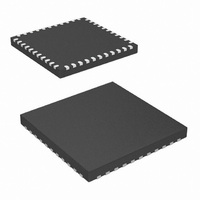
IC PIC MCU 128KB FLASH 44QFN
Manufacturer
Microchip Technology
Series
PIC® XLP™ 18Fr
Datasheets
1.PIC18LF24J10-ISS.pdf
(32 pages)
2.PIC18F26J13-ISS.pdf
(496 pages)
3.PIC18F26J13-ISS.pdf
(558 pages)
4.PIC18F26J13-ISS.pdf
(12 pages)
Specifications of PIC18F47J13-I/ML
Core Size
8-Bit
Program Memory Size
128KB (64K x 16)
Core Processor
PIC
Speed
48MHz
Connectivity
I²C, LIN, SPI, UART/USART
Peripherals
Brown-out Detect/Reset, POR, PWM, WDT
Number Of I /o
34
Program Memory Type
FLASH
Ram Size
3.8K x 8
Voltage - Supply (vcc/vdd)
2.15 V ~ 3.6 V
Data Converters
A/D 13x10b/12b
Oscillator Type
Internal
Operating Temperature
-40°C ~ 85°C
Package / Case
*
Controller Family/series
PIC18
Cpu Speed
48MHz
Digital Ic Case Style
QFN
Supply Voltage Range
1.8V To 5.5V
Embedded Interface Type
I2C, SPI, USART
Rohs Compliant
Yes
Processor Series
PIC18F
Core
PIC
Data Bus Width
8 bit
Data Ram Size
4 KB
Interface Type
I2C, SPI, EUSART
Maximum Clock Frequency
48 MHz
Number Of Programmable I/os
25
Number Of Timers
8
Operating Supply Voltage
2 V to 3.6 V
Maximum Operating Temperature
+ 85 C
Mounting Style
SMD/SMT
3rd Party Development Tools
52715-96, 52716-328, 52717-734, 52712-325, EWPIC18
Development Tools By Supplier
DM164128, DM180021, DM183026-2, DV164131, MA180030, DM183022, DM183032, DV164136, MA180024
Minimum Operating Temperature
- 40 C
On-chip Adc
12 bit, 13 Channel
Lead Free Status / RoHS Status
Lead free / RoHS Compliant
For Use With
MA180030 - BOARD DEMO PIC18F47J13 FS USBMA180029 - BOARD DEMO PIC18F47J53 FS USB
Eeprom Size
-
Lead Free Status / Rohs Status
Details


TABLE 1-3:
2010 Microchip Technology Inc.
RB4/CCP4/KBI0/SCL2/RP7
RB5/CCP5/KBI1/SDA2/RP8
RB6/CCP6/KBI2/PGC/RP9
RB7/CCP7/KBI3/PGD/RP10
Legend: TTL = TTL compatible input
Note 1:
RB4
CCP4
KBI0
SCL2
RP7
RB5
CCP5
KBI1
SDA2
RP8
RB6
CCP6
KBI2
PGC
RP9
RB7
CCP7
KBI3
PGD
RP10
2:
Pin Name
ST = Schmitt Trigger input with CMOS levels
I
P
DIG = Digital output
RA7 and RA6 will be disabled if OSC1 and OSC2 are used for the clock function.
5.5V tolerant.
= Input
= Power
PIC18F2XJ13 PINOUT I/O DESCRIPTIONS (CONTINUED)
28-SPDIP/
SSOP/
SOIC
25
26
27
28
Pin Number
(2)
(2)
(2)
(2)
28-QFN
22
23
24
25
(2)
(2)
(2)
(2)
Preliminary
Type
Pin
I/O
I/O
I/O
I/O
I/O
I/O
I/O
I/O
I/O
I/O
I/O
I/O
I/O
I/O
I/O
I
I
I
I
I
TTL/DIG
TTL/DIG
TTL/DIG
TTL/DIG
ST/DIG
ST/DIG
ST/DIG
ST/DIG
ST/DIG
ST/DIG
ST/DIG
ST/DIG
ST/DIG
Buffer
I
Type
2
TTL
TTL
TTL
TTL
PIC18F47J13 FAMILY
I
ST
C™
2
C
CMOS = CMOS compatible input or output
Analog = Analog input
O
OD
I
2
C™
PORTB (continued)
Digital I/O.
Capture/Compare/PWM input/output.
Interrupt-on-change pin.
I
Remappable Peripheral Pin 7 input/output.
Digital I/O.
Capture/Compare/PWM input/output.
Interrupt-on-change pin.
I
Remappable Peripheral Pin 8 input/output.
Digital I/O.
Capture/Compare/PWM input/output.
Interrupt-on-change pin.
ICSP™ clock input.
Remappable Peripheral Pin 9 input/output.
Digital I/O.
Capture/Compare/PWM input/output.
Interrupt-on-change pin.
In-Circuit Debugger and ICSP programming
data pin.
Remappable Peripheral Pin 10 input/output.
2
2
C clock input/output.
C data input/output.
= Output
= Open-Drain (no P diode to V
= Open-Drain, I
Description
2
C specific
DS39974A-page 19
DD
)
Related parts for PIC18F47J13-I/ML
Image
Part Number
Description
Manufacturer
Datasheet
Request
R

Part Number:
Description:
Manufacturer:
Microchip Technology Inc.
Datasheet:
Part Number:
Description:
Manufacturer:
Microchip Technology Inc.
Datasheet:
Part Number:
Description:
Manufacturer:
Microchip Technology Inc.
Datasheet:
Part Number:
Description:
Manufacturer:
Microchip Technology Inc.
Datasheet:
Part Number:
Description:
Manufacturer:
Microchip Technology Inc.
Datasheet:
Part Number:
Description:
Manufacturer:
Microchip Technology Inc.
Datasheet:
Part Number:
Description:
Manufacturer:
Microchip Technology Inc.
Datasheet:
Part Number:
Description:
Manufacturer:
Microchip Technology Inc.
Datasheet: