ATTINY461-20MU Atmel, ATTINY461-20MU Datasheet - Page 56
ATTINY461-20MU
Manufacturer Part Number
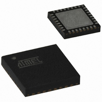
ATTINY461-20MU
Description
IC AVR MCU 4K 20MHZ 32-QFN
Manufacturer
Atmel
Series
AVR® ATtinyr
Specifications of ATTINY461-20MU
Core Processor
AVR
Core Size
8-Bit
Speed
20MHz
Connectivity
USI
Peripherals
Brown-out Detect/Reset, POR, PWM, WDT
Number Of I /o
16
Program Memory Size
4KB (2K x 16)
Program Memory Type
FLASH
Eeprom Size
256 x 8
Ram Size
256 x 8
Voltage - Supply (vcc/vdd)
2.7 V ~ 5.5 V
Data Converters
A/D 11x10b
Oscillator Type
Internal
Operating Temperature
-40°C ~ 85°C
Package / Case
32-VQFN Exposed Pad, 32-HVQFN, 32-SQFN, 32-DHVQFN
Processor Series
ATTINY4x
Core
AVR8
Data Bus Width
8 bit
Data Ram Size
256 B
Interface Type
2-Wire, SPI, USI
Maximum Clock Frequency
20 MHz
Number Of Programmable I/os
16
Number Of Timers
2
Maximum Operating Temperature
+ 85 C
Mounting Style
SMD/SMT
3rd Party Development Tools
EWAVR, EWAVR-BL
Development Tools By Supplier
ATAVRDRAGON, ATSTK500, ATSTK600, ATAVRISP2, ATAVRONEKIT
Minimum Operating Temperature
- 40 C
On-chip Adc
10 bit, 11 Channel
For Use With
ATSTK600-DIP40 - STK600 SOCKET/ADAPTER 40-PDIPATAVRBC100 - REF DESIGN KIT BATTERY CHARGER770-1007 - ISP 4PORT ATMEL AVR MCU SPI/JTAG
Lead Free Status / RoHS Status
Lead free / RoHS Compliant
Available stocks
Company
Part Number
Manufacturer
Quantity
Price
Company:

Part Number:
ATTINY461-20MU
Manufacturer:
KODENSHI
Quantity:
991
Company:
Part Number:
ATTINY461-20MUR
Manufacturer:
ATMEL
Quantity:
5 560


10.1
10.1.1
56
Ports as General Digital I/O
ATtiny261/461/861
Configuring the Pin
The ports are bi-directional I/O ports with optional internal pull-ups.
tional description of one I/O-port pin, here generically called Pxn.
Figure 10-2. General Digital I/O
Note:
Each port pin consists of three register bits: DDxn, PORTxn, and PINxn. As shown in
Description” on page
at the PORTx I/O address, and the PINxn bits at the PINx I/O address.
The DDxn bit in the DDRx Register selects the direction of this pin. If DDxn is written logic one,
Pxn is configured as an output pin. If DDxn is written logic zero, Pxn is configured as an input
pin.
If PORTxn is written logic one when the pin is configured as an input pin, the pull-up resistor is
activated. To switch the pull-up resistor off, PORTxn has to be written logic zero or the pin has to
Pxn
1. WRx, WPx, WDx, RRx, RPx, and RDx are common to all pins within the same port. clk
SLEEP, and PUD are common to all ports.
PUD:
SLEEP:
clk
I/O
:
69, the DDxn bits are accessed at the DDRx I/O address, the PORTxn bits
PULLUP DISABLE
SLEEP CONTROL
I/O CLOCK
SLEEP
(1)
SYNCHRONIZER
D
L
Q
Q
D
PINxn
Q
Q
RESET
RESET
PORTxn
WDx:
RDx:
WRx:
RRx:
RPx:
WPx:
Q
Q
Q
Q
DDxn
CLR
CLR
D
D
RRx
WRITE DDRx
READ DDRx
WRITE PORTx
READ PORTx REGISTER
READ PORTx PIN
WRITE PINx REGISTER
Figure 10-2
PUD
WDx
RDx
RPx
clk
1
0
I/O
WRx
shows a func-
2588E–AVR–08/10
WPx
“Register
I/O
,
Related parts for ATTINY461-20MU
Image
Part Number
Description
Manufacturer
Datasheet
Request
R

Part Number:
Description:
Manufacturer:
Atmel Corporation
Datasheet:
Part Number:
Description:
Manufacturer:
Atmel Corporation
Datasheet:

Part Number:
Description:
IC MCU AVR 4K FLASH 20MHZ 20SOIC
Manufacturer:
Atmel
Datasheet:

Part Number:
Description:
MCU AVR 4K FLASH 15MHZ 32-QFN
Manufacturer:
Atmel
Datasheet:
Part Number:
Description:
MCU AVR 4KB FLASH 15MHZ 32-VQFN
Manufacturer:
Atmel
Datasheet:
Part Number:
Description:
MCU AVR 4KB FLASH 20MHZ 20SOIC
Manufacturer:
Atmel
Datasheet:


Part Number:
Description:
IC MCU AVR 4K 20MHZ 32QFN
Manufacturer:
Atmel
Datasheet:

Part Number:
Description:
Microcontrollers (MCU) 4kB Flash 0.256kB EEPROM 16 I/O Pins
Manufacturer:
Atmel
Datasheet:
Part Number:
Description:
IC, MCU, 8BIT, 2K FLASH, 20SOIC
Manufacturer:
Atmel
Datasheet:

Part Number:
Description:
IC, MCU, 8BIT, 2K FLASH, 20PDIP
Manufacturer:
Atmel
Datasheet: