ATMEGA48-20PU Atmel, ATMEGA48-20PU Datasheet - Page 80
ATMEGA48-20PU
Manufacturer Part Number
ATMEGA48-20PU
Description
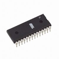
IC AVR MCU 4K 20MHZ 5V 28DIP
Manufacturer
Atmel
Series
AVR® ATmegar
Datasheets
1.ATAVRTS2080B.pdf
(378 pages)
2.ATMEGA48-20AU.pdf
(35 pages)
3.ATMEGA48-20PU.pdf
(377 pages)
Specifications of ATMEGA48-20PU
Core Processor
AVR
Core Size
8-Bit
Speed
20MHz
Connectivity
I²C, SPI, UART/USART
Peripherals
Brown-out Detect/Reset, POR, PWM, WDT
Number Of I /o
23
Program Memory Size
4KB (2K x 16)
Program Memory Type
FLASH
Eeprom Size
256 x 8
Ram Size
512 x 8
Voltage - Supply (vcc/vdd)
2.7 V ~ 5.5 V
Data Converters
A/D 6x10b
Oscillator Type
Internal
Operating Temperature
-40°C ~ 85°C
Package / Case
28-DIP (0.300", 7.62mm)
Processor Series
ATMEGA48x
Core
AVR8
Data Bus Width
8 bit
Data Ram Size
512 B
Interface Type
2-Wire/SPI/USART/Serial
Maximum Clock Frequency
20 MHz
Number Of Programmable I/os
23
Number Of Timers
3
Operating Supply Voltage
2.7 V to 5.5 V
Maximum Operating Temperature
+ 85 C
Mounting Style
Through Hole
3rd Party Development Tools
EWAVR, EWAVR-BL
Development Tools By Supplier
ATAVRDRAGON, ATSTK500, ATSTK600, ATAVRISP2, ATAVRONEKIT
Minimum Operating Temperature
- 40 C
On-chip Adc
6-ch x 10-bit
Cpu Family
ATmega
Device Core
AVR
Device Core Size
8b
Frequency (max)
20MHz
Total Internal Ram Size
512Byte
# I/os (max)
23
Number Of Timers - General Purpose
3
Operating Supply Voltage (typ)
3.3/5V
Operating Supply Voltage (max)
5.5V
Operating Supply Voltage (min)
2.7V
Instruction Set Architecture
RISC
Operating Temp Range
-40C to 85C
Operating Temperature Classification
Industrial
Mounting
Through Hole
Pin Count
28
Package Type
PDIP
For Use With
ATSTK600-TQFP32 - STK600 SOCKET/ADAPTER 32-TQFPATSTK600 - DEV KIT FOR AVR/AVR32770-1007 - ISP 4PORT ATMEL AVR MCU SPI/JTAGATAVRDRAGON - KIT DRAGON 32KB FLASH MEM AVRATAVRISP2 - PROGRAMMER AVR IN SYSTEMATJTAGICE2 - AVR ON-CHIP D-BUG SYSTEM
Lead Free Status / RoHS Status
Lead free / RoHS Compliant


13.3.2
80
ATmega48/88/168
Alternate Functions of Port C
Notes:
Table 13-5.
The Port C pins with alternate functions are shown in
Table 13-6.
The alternate pin configuration is as follows:
• RESET/PCINT14 – Port C, Bit 6
Signal
Name
PUOE
PUOV
DDOE
DDOV
PVOE
PVOV
DIEOE
DIEOV
DI
AIO
Port Pin
PC6
PC5
PC4
PC3
PC2
PC1
PC0
1. INTRC means that one of the internal RC Oscillators are selected (by the CKSEL fuses),
EXTCK means that external clock is selected (by the CKSEL fuses).
PB3/MOSI/
OC2/PCINT3
SPE • MSTR
PORTB3 • PUD
SPE • MSTR
0
SPE • MSTR +
OC2A ENABLE
SPI MSTR OUTPUT
+ OC2A
PCINT3 • PCIE0
1
PCINT3 INPUT
SPI SLAVE INPUT
–
Overriding Signals for Alternate Functions in PB3..PB0
Port C Pins Alternate Functions
Alternate Function
RESET (Reset pin)
PCINT14 (Pin Change Interrupt 14)
ADC5 (ADC Input Channel 5)
SCL (2-wire Serial Bus Clock Line)
PCINT13 (Pin Change Interrupt 13)
ADC4 (ADC Input Channel 4)
SDA (2-wire Serial Bus Data Input/Output Line)
PCINT12 (Pin Change Interrupt 12)
ADC3 (ADC Input Channel 3)
PCINT11 (Pin Change Interrupt 11)
ADC2 (ADC Input Channel 2)
PCINT10 (Pin Change Interrupt 10)
ADC1 (ADC Input Channel 1)
PCINT9 (Pin Change Interrupt 9)
ADC0 (ADC Input Channel 0)
PCINT8 (Pin Change Interrupt 8)
PB2/SS/
OC1B/PCINT2
SPE • MSTR
PORTB2 • PUD
SPE • MSTR
0
OC1B ENABLE
OC1B
PCINT2 • PCIE0
1
PCINT2 INPUT
SPI SS
–
Table
PB1/OC1A/
PCINT1
0
0
0
0
OC1A ENABLE
OC1A
PCINT1 • PCIE0
1
PCINT1 INPUT
–
13-6.
PB0/ICP1/
PCINT0
0
0
0
0
0
0
PCINT0 • PCIE0
1
PCINT0 INPUT
ICP1 INPUT
–
2545S–AVR–07/10
Related parts for ATMEGA48-20PU
Image
Part Number
Description
Manufacturer
Datasheet
Request
R

Part Number:
Description:
IC AVR MCU 4K 5V 20MHZ 32-TQFP
Manufacturer:
Atmel
Datasheet:

Part Number:
Description:
Manufacturer:
Atmel Corporation
Datasheet:
Part Number:
Description:
Manufacturer:
Atmel Corporation
Datasheet:
Part Number:
Description:
IC AVR MCU 4K 20MHZ 5V 32TQFP
Manufacturer:
Atmel
Datasheet:

Part Number:
Description:
IC AVR MCU 4K 20MHZ 5V 32-QFN
Manufacturer:
Atmel
Datasheet:

Part Number:
Description:
IC AVR MCU 4K 5V 20MHZ 32-TQFP
Manufacturer:
Atmel
Datasheet:

Part Number:
Description:
IC AVR MCU 4K 5V 20MHZ 32-QFN
Manufacturer:
Atmel
Datasheet:
Part Number:
Description:
IC AVR MCU 4K 5V 20MHZ 32-QFN
Manufacturer:
Atmel
Datasheet:

Part Number:
Description:
IC AVR MCU 4K 5V 20MHZ 28-DIP
Manufacturer:
Atmel
Datasheet:
Part Number:
Description:
IC AVR MCU 4K 5V 20MHZ 28-DIP
Manufacturer:
Atmel
Datasheet:

Part Number:
Description:
IC AVR MCU 4K FLASH 20MHZ 28QFN
Manufacturer:
Atmel
Datasheet:
Part Number:
Description:
MCU AVR 4KB FLASH 20MHZ 32QFN
Manufacturer:
Atmel
Datasheet: