ATTINY2313-20MU Atmel, ATTINY2313-20MU Datasheet - Page 56
ATTINY2313-20MU
Manufacturer Part Number
ATTINY2313-20MU
Description
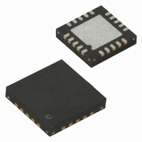
IC MCU AVR 2K FLASH 20MLF
Manufacturer
Atmel
Series
AVR® ATtinyr
Specifications of ATTINY2313-20MU
Core Processor
AVR
Core Size
8-Bit
Speed
20MHz
Connectivity
SPI, UART/USART
Peripherals
Brown-out Detect/Reset, POR, PWM, WDT
Number Of I /o
18
Program Memory Size
2KB (1K x 16)
Program Memory Type
FLASH
Eeprom Size
128 x 8
Ram Size
128 x 8
Voltage - Supply (vcc/vdd)
2.7 V ~ 5.5 V
Oscillator Type
Internal
Operating Temperature
-40°C ~ 85°C
Package / Case
20-MLF®, QFN
Processor Series
ATTINY2x
Core
AVR8
Data Bus Width
8 bit
Data Ram Size
128 B
Interface Type
SPI/UART/USI
Maximum Clock Frequency
20 MHz
Number Of Programmable I/os
18
Number Of Timers
2
Operating Supply Voltage
2.7 V to 5.5 V
Maximum Operating Temperature
+ 85 C
Mounting Style
SMD/SMT
3rd Party Development Tools
EWAVR, EWAVR-BL
Development Tools By Supplier
ATAVRDRAGON, ATSTK500, ATSTK600, ATAVRISP2, ATAVRONEKIT
Minimum Operating Temperature
- 40 C
Package
20MLF EP
Device Core
AVR
Family Name
ATtiny
Maximum Speed
20 MHz
For Use With
ATSTK600-DIP40 - STK600 SOCKET/ADAPTER 40-PDIP770-1007 - ISP 4PORT ATMEL AVR MCU SPI/JTAGATAVRDRAGON - KIT DRAGON 32KB FLASH MEM AVRATAVRISP2 - PROGRAMMER AVR IN SYSTEMATJTAGICE2 - AVR ON-CHIP D-BUG SYSTEM
Lead Free Status / RoHS Status
Lead free / RoHS Compliant
Data Converters
-
Lead Free Status / Rohs Status
Lead free / RoHS Compliant
Other names
Q2312268A
Available stocks
Company
Part Number
Manufacturer
Quantity
Price

Part Number:
ATTINY2313-20MU
Manufacturer:
原装ATMEL
Quantity:
20 000


Alternate Functions of
Port D
56
ATtiny2313
The Port D pins with alternate functions are shown in
Table 28. Port D Pins Alternate Functions
The alternate pin configuration is as follows:
• ICP – Port D, Bit 6
ICP: Timer/Counter1 Input Capture Pin. The PD6 pin can act as an Input Capture pin for
Timer/Counter1
• OC0B/T1 – Port D, Bit 5
OC0B: Output Compare Match B output: The PD5 pin can serve as an external output for the
Timer/Counter0 Output Compare B. The pin has to be configured as an output (DDD5 set (one))
to serve this function. The OC0B pin is also the output pin for the PWM mode timer function.
T1: Timer/Counter1 External Counter Clock input is enabled by setting (one) the bits CS02 and
CS01 in the Timer/Counter1 Control Register (TCCR1).
• T0 – Port D, Bit 4
T0: Timer/Counter0 External Counter Clock input is enabled by setting (one) the bits CS02 and
CS01 in the Timer/Counter0 Control Register (TCCR0).
• INT1 – Port D, Bit 3
INT1: External Interrupt Source 1. The PD3 pin can serve as an external interrupt source to the
MCU.
• INT0/XCK/CKOUT – Port D, Bit 2
INT0: External Interrupt Source 0. The PD2 pin can serve as en external interrupt source to the
MCU.
XCK: USART Transfer Clock used only by Synchronous Transfer mode.
CKOUT: System Clock Output
• TXD – Port D, Bit 1
TXD: UART Data Transmitter.
• RXD – Port D, Bit 0
RXD: UART Data Receiver.
Port Pin
PD6
PD5
PD4
PD3
PD2
PD1
PD0
Alternate Function
ICP
OC0B/T1
T0
INT1
INT0/XCK/CKOUT
TXD
RXD
Table
28.
2543L–AVR–08/10
Related parts for ATTINY2313-20MU
Image
Part Number
Description
Manufacturer
Datasheet
Request
R

Part Number:
Description:
IC, MCU, 8BIT, 2K FLASH, 20SOIC
Manufacturer:
Atmel
Datasheet:

Part Number:
Description:
IC, MCU, 8BIT, 2K FLASH, 20PDIP
Manufacturer:
Atmel
Datasheet:
Part Number:
Description:
IC, MCU, 8BIT, 8K FLASH, 20PDIP
Manufacturer:
Atmel
Datasheet:
Part Number:
Description:
IC, MCU, 8BIT, 8K FLASH, 20SOIC
Manufacturer:
Atmel
Datasheet:

Part Number:
Description:
DEV KIT FOR AVR/AVR32
Manufacturer:
Atmel
Datasheet:

Part Number:
Description:
INTERVAL AND WIPE/WASH WIPER CONTROL IC WITH DELAY
Manufacturer:
ATMEL Corporation
Datasheet:
Part Number:
Description:
Low-Voltage Voice-Switched IC for Hands-Free Operation
Manufacturer:
ATMEL Corporation
Datasheet:
Part Number:
Description:
MONOLITHIC INTEGRATED FEATUREPHONE CIRCUIT
Manufacturer:
ATMEL Corporation
Datasheet:
Part Number:
Description:
AM-FM Receiver IC U4255BM-M
Manufacturer:
ATMEL Corporation
Datasheet:
Part Number:
Description:
Monolithic Integrated Feature Phone Circuit
Manufacturer:
ATMEL Corporation
Datasheet:
Part Number:
Description:
Multistandard Video-IF and Quasi Parallel Sound Processing
Manufacturer:
ATMEL Corporation
Datasheet:
Part Number:
Description:
High-performance EE PLD
Manufacturer:
ATMEL Corporation
Datasheet: