PIC24F04KA201-I/P Microchip Technology, PIC24F04KA201-I/P Datasheet - Page 9
PIC24F04KA201-I/P
Manufacturer Part Number
PIC24F04KA201-I/P
Description
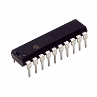
IC PIC MCU FLASH 512KX4 20-PDIP
Manufacturer
Microchip Technology
Series
PIC® XLP™ 24Fr
Datasheets
1.PIC24F04KA201-ISS.pdf
(8 pages)
2.PIC24F04KA201-ISS.pdf
(48 pages)
3.PIC24F04KA201-ISS.pdf
(224 pages)
4.PIC24F04KA201-ISS.pdf
(26 pages)
Specifications of PIC24F04KA201-I/P
Core Size
16-Bit
Program Memory Size
4KB (1.375K x 24)
Peripherals
Brown-out Detect/Reset, HLVD, POR, PWM, WDT
Core Processor
PIC
Speed
32MHz
Connectivity
I²C, IrDA, SPI, UART/USART
Number Of I /o
18
Program Memory Type
FLASH
Ram Size
512 x 8
Voltage - Supply (vcc/vdd)
1.8 V ~ 3.6 V
Data Converters
A/D 9x10b
Oscillator Type
Internal
Operating Temperature
-40°C ~ 85°C
Package / Case
20-DIP (0.300", 7.62mm)
Controller Family/series
PIC24
No. Of I/o's
18
Ram Memory Size
512Byte
Cpu Speed
32MHz
No. Of Timers
3
Processor Series
PIC24F
Core
PIC
Data Bus Width
16 bit
Data Ram Size
512 B
Interface Type
I2C, SPI, UART
Maximum Clock Frequency
32 KHz
Number Of Programmable I/os
12
Number Of Timers
3
Operating Supply Voltage
1.8 V to 3.6 V
Maximum Operating Temperature
+ 125 C
Mounting Style
Through Hole
3rd Party Development Tools
52713-733, 52714-737, 53276-922, EWDSPIC
Development Tools By Supplier
PG164130, DV164035, DV244005, DV164005, DM240001
Minimum Operating Temperature
- 40 C
On-chip Adc
10 bit, 9 Channel
Lead Free Status / RoHS Status
Lead free / RoHS Compliant
Eeprom Size
-
Lead Free Status / Rohs Status
Details


3.5
To erase the program memory (all of code memory,
data memory and Configuration bits, including the
code-protect bits), set the NVMCON to 4064h and then
execute the programming cycle.
Figure 3-6
for Bulk Erase. This process includes the ICSP
command code, which must be transmitted (for each
instruction), LSB first, using the PGCx and PGDx pins
(see
Table 3-4
instruction for the Bulk Erase mode.
TABLE 3-4:
2010 Microchip Technology Inc.
Step 1: Exit the Reset vector.
Step 2: Set the NVMCON to erase the entire program memory.
Step 3: Set the TBLPAG and perform dummy table write to select the erased memory.
Step 4: Initiate the erase cycle.
Step 5: Repeat this step to poll the WR bit (bit 15 of NVMCON) until it is cleared by the hardware.
Note:
Command
(Binary)
Figure
0000
0000
0000
0000
0000
0000
0000
0000
0000
0000
0000
0000
0000
0000
0000
0000
0000
0000
0000
0000
0001
0000
Erasing Program Memory
provides the steps for executing serial
illustrates the ICSP programming process
Program memory must be erased before
writing any data to program memory.
3-2).
SERIAL INSTRUCTION EXECUTION FOR CHIP ERASE
000000
040200
000000
24064A
883B0A
200000
880190
200000
BB0800
000000
000000
A8E761
000000
000000
000000
040200
000000
803B02
883C22
000000
<VISI>
000000
(Hex)
Data
NOP
GOTO
NOP
MOV
MOV
MOV
MOV
MOV
TBLWTL W0, [W0]
NOP
NOP
BSET
NOP
NOP
NOP
GOTO
NOP
MOV
MOV
NOP
Clock out the contents of the VISI register.
NOP
0x200
#0x4064, W10
W10, NVMCON
#<PAGEVAL>, W0
W0, TBLPAG
#0x0000, W0
NVMCON, #WR
0x200
NVMCON, W2
W2, VISI
FIGURE 3-6:
Description
PIC24FXXKA2XX
Set the WR bit to Initiate Erase
Write 4064h to NVMCON SFR
Delay P11 + P10 Time
BULK ERASE FLOW
Start
End
DS39991A-page 9
Related parts for PIC24F04KA201-I/P
Image
Part Number
Description
Manufacturer
Datasheet
Request
R

Part Number:
Description:
Manufacturer:
Microchip Technology Inc.
Datasheet:
Part Number:
Description:
Manufacturer:
Microchip Technology Inc.
Datasheet:
Part Number:
Description:
Manufacturer:
Microchip Technology Inc.
Datasheet:
Part Number:
Description:
Manufacturer:
Microchip Technology Inc.
Datasheet:
Part Number:
Description:
Manufacturer:
Microchip Technology Inc.
Datasheet:
Part Number:
Description:
Manufacturer:
Microchip Technology Inc.
Datasheet:
Part Number:
Description:
Manufacturer:
Microchip Technology Inc.
Datasheet:
Part Number:
Description:
Manufacturer:
Microchip Technology Inc.
Datasheet: