PIC24F04KA201-I/P Microchip Technology, PIC24F04KA201-I/P Datasheet - Page 16
PIC24F04KA201-I/P
Manufacturer Part Number
PIC24F04KA201-I/P
Description
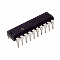
IC PIC MCU FLASH 512KX4 20-PDIP
Manufacturer
Microchip Technology
Series
PIC® XLP™ 24Fr
Datasheets
1.PIC24F04KA201-ISS.pdf
(8 pages)
2.PIC24F04KA201-ISS.pdf
(48 pages)
3.PIC24F04KA201-ISS.pdf
(224 pages)
4.PIC24F04KA201-ISS.pdf
(26 pages)
Specifications of PIC24F04KA201-I/P
Core Size
16-Bit
Program Memory Size
4KB (1.375K x 24)
Peripherals
Brown-out Detect/Reset, HLVD, POR, PWM, WDT
Core Processor
PIC
Speed
32MHz
Connectivity
I²C, IrDA, SPI, UART/USART
Number Of I /o
18
Program Memory Type
FLASH
Ram Size
512 x 8
Voltage - Supply (vcc/vdd)
1.8 V ~ 3.6 V
Data Converters
A/D 9x10b
Oscillator Type
Internal
Operating Temperature
-40°C ~ 85°C
Package / Case
20-DIP (0.300", 7.62mm)
Controller Family/series
PIC24
No. Of I/o's
18
Ram Memory Size
512Byte
Cpu Speed
32MHz
No. Of Timers
3
Processor Series
PIC24F
Core
PIC
Data Bus Width
16 bit
Data Ram Size
512 B
Interface Type
I2C, SPI, UART
Maximum Clock Frequency
32 KHz
Number Of Programmable I/os
12
Number Of Timers
3
Operating Supply Voltage
1.8 V to 3.6 V
Maximum Operating Temperature
+ 125 C
Mounting Style
Through Hole
3rd Party Development Tools
52713-733, 52714-737, 53276-922, EWDSPIC
Development Tools By Supplier
PG164130, DV164035, DV244005, DV164005, DM240001
Minimum Operating Temperature
- 40 C
On-chip Adc
10 bit, 9 Channel
Lead Free Status / RoHS Status
Lead free / RoHS Compliant
Eeprom Size
-
Lead Free Status / Rohs Status
Details


PIC24FXXKA2XX
TABLE 3-8:
DS39991A-page 16
FWPSA
FWDTEN
GSS0
GWRP
ICS<1:0>
IESO
MCLRE
OSCIOFNC
POSCMD<1:0>
POSCFREQ<1:0> FOSC<4:3>
PWRTEN
SOSCSEL
Note 1:
Bit Field
(1)
The MCLRE fuse can only be changed when using the V
from accidentally locking out the device from low-voltage test entry.
PIC24FXXKA2XX FAMILY CONFIGURATION BITS DESCRIPTION (CONTINUED)
FWDT<4>
FWDT<7>
FGS<1>
FGS<0>
FICD<1:0>
FOSCSEL<7>
FPOR<7>
FOSC<2>
FOSC<1:0>
FPOR<3>
FOSC<5>
Register
WDT Prescaler
1 = WDT prescaler ratio of 1:128
0 = WDT prescaler ratio of 1:32
Watchdog Timer Enable bit
1 = WDT is enabled
0 = WDT is disabled (control is placed on the SWDTEN bit)
General Segment Code Flash Code Protection bit
1 = No protection
0 = Standard security is enabled
General Segment Code Flash Write Protection bit
1 = General segment may be written
0 = General segment is write-protected
ICD Pin Placement Select bit
11 = Reserved; do not use
10 = PGEC2/PGED2 are used for ICSP programming
01 = PGEC3/PGED3 are used for ICSP programming
00 = Reserved; do not use
Internal External Switchover bit
1 = Internal External Switchover mode is enabled (Two-Speed Start-up
0 = Internal External Switchover mode is disabled (Two-Speed Start-up disabled)
MCLR Pin Enable bit
1 = MCLR pin is enabled; RA5 input pin is disabled
0 = RA5 input pin is enabled; MCLR is disabled
CLKO Enable Configuration bit
1 = CLKO output signal is active on the OSCO pin; primary oscillator must be
0 = CLKO output is disabled
Primary Oscillator Configuration bits
11 = Primary oscillator disabled
10 = HS Oscillator mode selected (4 MHz-25 MHz)
01 = XT Oscillator mode selected (100 kHz-4 MHz)
00 = External Clock mode selected
Primary Oscillator Frequency Range Configuration bits
11 = Primary oscillator/external clock input frequency is greater than 8 MHz
10 = Primary oscillator/external clock input frequency is between 100 kHz and
01 = Primary oscillator/external clock input frequency is less than 100 kHz
00 = Reserved; do not use
Power-up Timer Enable bit
0 = PWRT is disabled
1 = PWRT is enabled
Secondary Oscillator Select bit
1 = Secondary oscillator is configured for high-power operation
0 = Secondary oscillator is configured for low-power operation
enabled)
disabled or configured for the External Clock mode (EC) for the CLKO to
be active (POSCMD<1:0> = 11 or 00)
8 MHz
(1)
PP
-Based Test mode entry. This prevents a user
Description
2010 Microchip Technology Inc.
Related parts for PIC24F04KA201-I/P
Image
Part Number
Description
Manufacturer
Datasheet
Request
R

Part Number:
Description:
Manufacturer:
Microchip Technology Inc.
Datasheet:
Part Number:
Description:
Manufacturer:
Microchip Technology Inc.
Datasheet:
Part Number:
Description:
Manufacturer:
Microchip Technology Inc.
Datasheet:
Part Number:
Description:
Manufacturer:
Microchip Technology Inc.
Datasheet:
Part Number:
Description:
Manufacturer:
Microchip Technology Inc.
Datasheet:
Part Number:
Description:
Manufacturer:
Microchip Technology Inc.
Datasheet:
Part Number:
Description:
Manufacturer:
Microchip Technology Inc.
Datasheet:
Part Number:
Description:
Manufacturer:
Microchip Technology Inc.
Datasheet: