PIC24F04KA201-I/P Microchip Technology, PIC24F04KA201-I/P Datasheet - Page 3
PIC24F04KA201-I/P
Manufacturer Part Number
PIC24F04KA201-I/P
Description
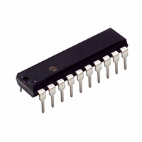
IC PIC MCU FLASH 512KX4 20-PDIP
Manufacturer
Microchip Technology
Series
PIC® XLP™ 24Fr
Datasheets
1.PIC24F04KA201-ISS.pdf
(8 pages)
2.PIC24F04KA201-ISS.pdf
(48 pages)
3.PIC24F04KA201-ISS.pdf
(224 pages)
4.PIC24F04KA201-ISS.pdf
(26 pages)
Specifications of PIC24F04KA201-I/P
Core Size
16-Bit
Program Memory Size
4KB (1.375K x 24)
Peripherals
Brown-out Detect/Reset, HLVD, POR, PWM, WDT
Core Processor
PIC
Speed
32MHz
Connectivity
I²C, IrDA, SPI, UART/USART
Number Of I /o
18
Program Memory Type
FLASH
Ram Size
512 x 8
Voltage - Supply (vcc/vdd)
1.8 V ~ 3.6 V
Data Converters
A/D 9x10b
Oscillator Type
Internal
Operating Temperature
-40°C ~ 85°C
Package / Case
20-DIP (0.300", 7.62mm)
Controller Family/series
PIC24
No. Of I/o's
18
Ram Memory Size
512Byte
Cpu Speed
32MHz
No. Of Timers
3
Processor Series
PIC24F
Core
PIC
Data Bus Width
16 bit
Data Ram Size
512 B
Interface Type
I2C, SPI, UART
Maximum Clock Frequency
32 KHz
Number Of Programmable I/os
12
Number Of Timers
3
Operating Supply Voltage
1.8 V to 3.6 V
Maximum Operating Temperature
+ 125 C
Mounting Style
Through Hole
3rd Party Development Tools
52713-733, 52714-737, 53276-922, EWDSPIC
Development Tools By Supplier
PG164130, DV164035, DV244005, DV164005, DM240001
Minimum Operating Temperature
- 40 C
On-chip Adc
10 bit, 9 Channel
Lead Free Status / RoHS Status
Lead free / RoHS Compliant
Eeprom Size
-
Lead Free Status / Rohs Status
Details


2.2
The program memory map extends from 000000h to
FFFFFEh. Code storage is located at the base of the
memory map, and supports up to about 1.38 K words
of instructions (about 4 Kbytes).
memory map.
Table 2-2
number of program memory rows present in each
device variant.
The erase operation can be done on one word, half of
a row or one row at a time. The program operation can
be done only one word at a time.
The device Configuration registers are implemented
from location, F80000h to F80010h, and can be erased
or programmed one register at a time.
vides the implemented Configuration registers and
their locations.
Locations, FF0000h and FF0002h, are reserved for the
Device ID registers. These bits can be used by the
programmer to identify the device type that is being
programmed. See
information. The Device ID registers read out normally
even after code protection is applied.
TABLE 2-2:
TABLE 2-3:
2010 Microchip Technology Inc.
PIC24F04KA200
PIC24F04KA201
FGS
FOSCSEL
FOSC
FWDT
FPOR
FICD
FDS
Configuration Register
Device
Memory Map
provides the program memory size and
PROGRAM MEMORY SIZES
CONFIGURATION REGISTER
LOCATIONS
Section 4.0 “Device ID”
(Instruction Words)
Program Memory
Upper Address
AFEh (1.375K)
Figure 2-2
Address
F8000A
F8000C
F8000E
F80004
F80006
F80008
F80010
Table 2-3
depicts the
for more
Rows
44
pro-
FIGURE 2-2:
PIC24FXXKA2XX
Configuration Registers
Diagnostic Words
(2816 x 24-bit)
Code Memory
User Flash
(2 x 16-bit)
Device ID
Reserved
Reserved
Reserved
Reserved
PROGRAM MEMORY MAP
DS39991A-page 3
000AFEh
000000h
800000h
8007EEh
8007F0h
8007FEh
800800h
FEFFFEh
FF0000h
FF0002h
FF0004h
FFFFFEh
F80000h
F80010h
Related parts for PIC24F04KA201-I/P
Image
Part Number
Description
Manufacturer
Datasheet
Request
R

Part Number:
Description:
Manufacturer:
Microchip Technology Inc.
Datasheet:
Part Number:
Description:
Manufacturer:
Microchip Technology Inc.
Datasheet:
Part Number:
Description:
Manufacturer:
Microchip Technology Inc.
Datasheet:
Part Number:
Description:
Manufacturer:
Microchip Technology Inc.
Datasheet:
Part Number:
Description:
Manufacturer:
Microchip Technology Inc.
Datasheet:
Part Number:
Description:
Manufacturer:
Microchip Technology Inc.
Datasheet:
Part Number:
Description:
Manufacturer:
Microchip Technology Inc.
Datasheet:
Part Number:
Description:
Manufacturer:
Microchip Technology Inc.
Datasheet: